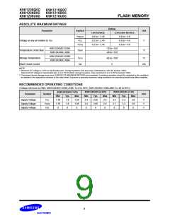
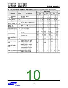
K9K1208Q0C
K9K1208D0C
K9K1208U0C
K9K1216Q0C
K9K1216D0C
K9K1216U0C
FLASH MEMORY
PRODUCT INTRODUCTION
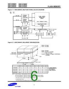
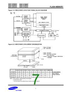
The K9K12XXX0C is a 528Mbit(553,648,218 bit) memory organized as 131,072 rows(pages) by 528(X8 device) or 264(X16 device)
columns. Spare eight columns are located from column address of 512~527(X8 device) or 256~263(X16 device). A 528-byte(X8
device) or 264-word(X16 device) data register is connected to memory cell arrays accommodating data transfer between the I/O buff-
ers and memory during page read and page program operations. The memory array is made up of 16 cells that are serially con-
nected to form a NAND structure. Each of the 16 cells resides in a different page. A block consists of two NAND structured strings. A
NAND structure consists of 16 cells. Total 135168 NAND cells reside in a block. The array organization is shown in Figure 2-1,2-2.
The program and read operations are executed on a page basis, while the erase operation is executed on a block basis. The memory
array consists of 4096 separately erasable 16K-Byte(X8 device) or 8K-Word(X16 device) blocks. It indicates that the bit by bit erase
operation is prohibited on the K9K12XXX0C.
The K9K12XXX0C has addresses multiplexed into 8 I/Os(X16 device case : lower 8 I/Os). K9K1216X0C allows sixteen bit wide data
transport into and out of page registers. This scheme dramatically reduces pin counts while providing high performance and allows
systems upgrades to future densities by maintaining consistency in system board design. Command, address and data are all written
through I/O′s by bringing WE to low while CE is low. Data is latched on the rising edge of WE. Command Latch Enable(CLE) and
Address Latch Enable(ALE) are used to multiplex command and address respectively, via the I/O pins. Some commands require one
bus cycle. For example, Reset command, Read command, Status Read command, etc require just one cycle bus. Some other com-
mands like Page Program and Copy-back Program and Block Erase, require three cycles: one cycle for setup and the other cycle for
execution. The 32M-byte(X8 device) or 16M-word(X16 device) physical space requires 25 addresses(X8 device) or 24
addresses(X16 device), thereby requiring four cycles for word-level addressing: column address, low row address and high row
address, in that order. Page Read and Page Program need the same four address cycles following the required command input. In
Block Erase operation, however, only the three row address cycles are used. Device operations are selected by writing specific com-
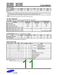
mands into the command register. Table 1 defines the specific commands of the K9K12XXX0C.
The device includes one block sized OTP(One Time Programmable), which can be used to increase system security or to provide
identification capabilities. Detailed information can be obtained by contact with Samsung.
Table 1. COMMAND SETS
Function
1st. Cycle
00h/01h(1)
50h
2nd. Cycle
Acceptable Command during Busy
Read 1
Read 2
Read ID
Reset
-
-
90h
-
FFh
-
10h
8Ah
-
O
Page Program
Copy-Back Program
Lock
80h
00h
2Ah
Unlock
23h
24h
-
Lock-tight
2Ch
Read Block Lock Status
Block Erase
Read Status
7Ah
-
60h
D0h
-
70h
O
NOTE : 1. The 01h command is available only on X8 device(K9K1208X0C).
Caution : Any undefined command inputs are prohibited except for above command set of Table 1.
8

 SAMSUNG [ SAMSUNG ]