K9K1208Q0C
K9K1208D0C
K9K1208U0C
K9K1216Q0C
K9K1216D0C
K9K1216U0C
FLASH MEMORY
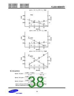
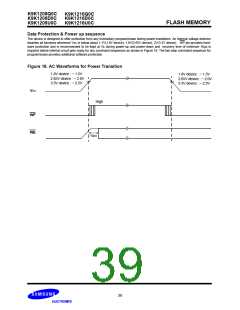
Data Protection & Power up sequence
The device is designed to offer protection from any involuntary program/erase during power-transitions. An internal voltage detector
disables all functions whenever Vcc is below about 1.1V(1.8V device), 1.8V(2.65V device), 2V(3.3V device). WP pin provides hard-
ware protection and is recommended to be kept at VIL during power-up and power-down and recovery time of minimum 10µs is
required before internal circuit gets ready for any command sequences as shown in Figure 18. The two step command sequence for
program/erase provides additional software protection.
Figure 18. AC Waveforms for Power Transition
1.8V device : ~ 1.5V
2.65V device : ~ 2.0V
3.3V device : ~ 2.5V
1.8V device : ~ 1.5V
2.65V device : ~ 2.0V
3.3V device : ~ 2.5V
VCC
High
WP
WE
10µs
39

 SAMSUNG [ SAMSUNG ]