K9K1208Q0C
K9K1208D0C
K9K1208U0C
K9K1216Q0C
K9K1216D0C
K9K1216U0C
FLASH MEMORY
64M x 8 Bit / 32M x 16 Bit NAND Flash Memory
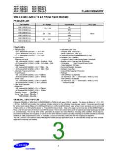
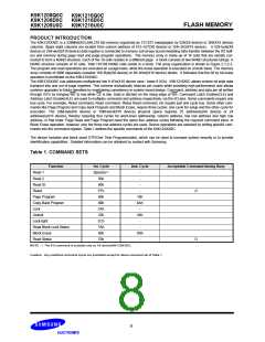
PRODUCT LIST.
Part Number
Vcc Range
Organization
PKG Type
K9K1208Q0C-G,J
K9K1216Q0C-G,J
K9K1208D0C-G,J
K9K1216D0C-G,J
K9K1208U0C-G,J
K9K1216U0C-G,J
X8
X16
X8
1.70 ~ 1.95V
2.4 ~ 2.9V
2.7 ~ 3.6V
FBGA
X16
X8
X16
FEATURES
• Voltage Supply
• Fast Write Cycle Time
- 1.8V device(K9K12XXQ0C) : 1.70~1.95V
- 2.65V device(K9F12XXD0C) : 2.4~2.9V
- 3.3V device(K9K12XXU0C) : 2.7 ~ 3.6 V
• Organization
- Program time : 200µs(Typ.)
- Block Erase Time : 2ms(Typ.)
• Command/Address/Data Multiplexed I/O Port
• Hardware Data Protection
- Memory Cell Array
- Program/Erase Lockout During Power Transitions
- X8 device(K9K1208X0C) : (64M + 2048K)bit x 8 bit
- X16 device(K9K1216X0C) : (32M + 1024 K)bit x 16bit
- Data Register
- X8 device(K9K1208X0C) : (512 + 16)bit x 8bit
- X16 device(K9K1216X0C) : (256 + 8)bit x16bit
• Automatic Program and Erase
• Reliable CMOS Floating-Gate Technology
- Endurance
: 100K Program/Erase Cycles
- Data Retention : 10 Years
• Command Register Operation
• Intelligent Copy-Back
• Unique ID for Copyright Protection
• Package
- Page Program
- X8 device(K9K1208X0C) : (512 + 16)Byte
- X16 device(K9K1216X0C) : (256 + 8)Word
- Block Erase :
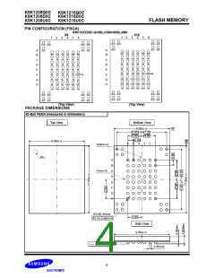
- K9K12XXX0C-GCB0/GIB0
63- Ball FBGA ( 9 x 11 /0.8mm pitch , Width 1.2 mm)
- K9K12XXX0C-JCB0/JIB0
- X8 device(K9K1208X0C) : (16K + 512)Byte
- X16 device(K9K1216X0C) : ( 8K + 256)Word
• Page Read Operation
63- Ball FBGA ( 9 x 11 /0.8mm pitch , Width 1.2 mm)
- Pb-free Package
- Page Size
- X8 device(K9K1208X0C) : (512 + 16)Byte
- X16 device(K9K1216X0C) : (256 + 8)Word
- Random Access
: 10µs(Max.)
- Serial Page Access : 50ns(Min.)*
*K9K1216Q0C : 60ns(Min.)
GENERAL DESCRIPTION
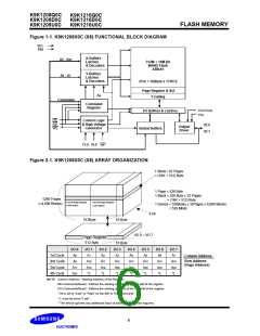
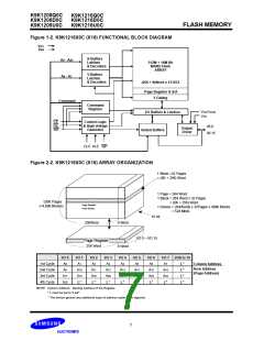
Offered in 64Mx8bit or 32Mx16bit, the K9K12XXX0C is 512M bit with spare 16M bit capacity. The device is offered in 1.8V, 2.65V,
3.3V Vcc. Its NAND cell provides the most cost-effective solutIon for the solid state mass storage market. A program operation can
be performed in typical 200µs on the 528-byte(X8 device) or 264-word(X16 device) page and an erase operation can be performed
in typical 2ms on a 16K-byte(X8 device) or 8K-word(X16 device) block. Data in the page can be read out at 50ns(K9K1216Q0C :
60ns) cycle time per byte (X8 device) or word(X16 device). The I/O pins serve as the ports for address and data input/output as well
as command input. The on-chip write control automates all program and erase functions including pulse repetition, where required,
and internal verification and margining of data. Even the write-intensive systems can take advantage of the K9K12XXX0C′s extended
reliability of 100K program/erase cycles by providing ECC(Error Correcting Code) with real time mapping-out algorithm.
The K9K12XXX0C is an optimum solution for large nonvolatile storage applications such as solid state file storage and other portable
applications requiring non-volatility.
3

 SAMSUNG [ SAMSUNG ]