K9K1208Q0C
K9K1208D0C
K9K1208U0C
K9K1216Q0C
K9K1216D0C
K9K1216U0C
FLASH MEMORY
Document Title
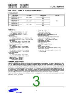
64M x 8 Bit , 32M x 16 Bit NAND Flash Memory
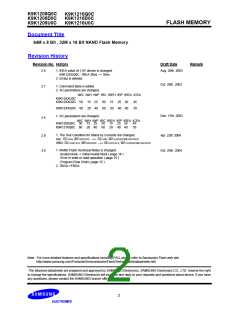
Revision History
Revision No. History
Draft Date
Remark
2.6
1. tREA value of 1.8V device is changed.
K9K12XXQ0C : tREA 30ns --> 35ns
2. Errata is deleted.
Aug. 20th. 2003
Oct. 28th. 2003
2.7
1. Command table is edited.
2. AC parameters are changed.
tWC tWH tWP tRC tREH tRP tREA tCEA
K9K12XXU0C
K9K12XXD0C 50 15 25 50 15 25 30
45
55
K9K12XXQ0C 60 20 40 60 20 40 40
1. AC parameters are changed.
Dec. 17th. 2003
2.8
tWC tWH tWP tRC tREH tRP tREA tCEA
K9K1208Q0C 50 15 25 50 15 25 35
K9K1216Q0C 60 20 40 60 20 40 40
45
55
1. The Test Condition for Stand-by Currents are changed.
ISB1: CE=VIH, WP=0V/VCC -->> CE=VIH, WP=LOCKPRE=0V/VCC
ISB2: CE=VCC-0.2, WP=0V/VCC -->> CE=VCC-0.2, WP=LOCKPRE=0V/VCC
Apr. 22th 2004
Oct. 25th. 2004
2.9
3.0
1. NAND Flash Technical Notes is changed.
-Invalid block -> initial invalid block ( page 14 )
-Error in write or read operation ( page 15 )
-Program Flow Chart ( page 15 )
2. TBGA->FBGA
Note : For more detailed features and specifications including FAQ, please refer to Samsung’s Flash web site.
http://www.samsung.com/Products/Semiconductor/Flash/TechnicalInfo/datasheets.htm
The attached datasheets are prepared and approved by SAMSUNG Electronics. SAMSUNG Electronics CO., LTD. reserve the right
to change the specifications. SAMSUNG Electronics will evaluate and reply to your requests and questions about device. If you have
any questions, please contact the SAMSUNG branch office near you.
2

 SAMSUNG [ SAMSUNG ]