K9F1208D0A K9F1216D0A
K9F1208U0A K9F1216U0A
FLASH MEMORY
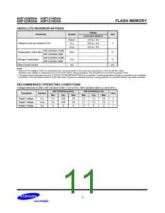
ABSOLUTE MAXIMUM RATINGS
Rating
3.3V/2.65V DEVICE
-0.6 to + 4.6
Parameter
Symbol
Unit
V
VIN/OUT
VCC
Voltage on any pin relative to VSS
-0.6 to + 4.6
VCCQ
-0.6 to + 4.6
K9F12XXX0A-XCB0
Temperature Under Bias
TBIAS
°C
K9F12XXX0A-XIB0
K9F12XXX0A-XCB0
Storage Temperature
TSTG
Ios
°C
K9F12XXX0A-XIB0
Short Circuit Current
mA
NOTE :
1. Minimum DC voltage is -0.6V on input/output pins. During transitions, this level may undershoot to -2.0V for periods <30ns.
Maximum DC voltage on input/output pins is VCC,+0.3V which, during transitions, may overshoot to VCC+2.0V for periods <20ns.
2. Permanent device damage may occur if ABSOLUTE MAXIMUM RATINGS are exceeded. Functional operation should be restricted to the conditions
as detailed in the operational sections of this data sheet. Exposure to absolute maximum rating conditions for extended periods may affect reliability.
RECOMMENDED OPERATING CONDITIONS
(Voltage reference to GND, K9F12XXX0A-XCB0 :TA=0 to 70°C, K9F12XXX0A-XIB0:TA=-40 to 85°C)
K9F12XXD0A(2.65V)
K9F12XXU0A(3.3V)
Parameter
Symbol
Unit
Min
Typ.
2.65
2.65
0
Max
Min
Typ.
3.3
3.3
0
Max
Supply Voltage
Supply Voltage
Supply Voltage
VCC
VCCQ
VSS
2.4
2.4
0
2.9
2.9
0
2.7
2.7
0
3.6
3.6
0
V
V
V
11

 SAMSUNG [ SAMSUNG ]