K9F1208D0A K9F1216D0A
K9F1208U0A K9F1216U0A
FLASH MEMORY
Product Introduction
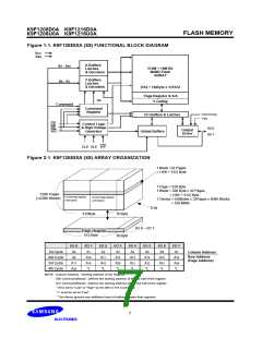
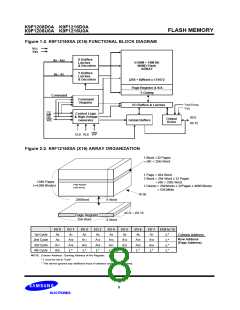
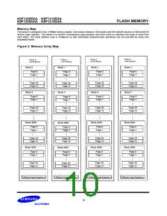
The K9F1208X0A is a 528Mbit(553,648,218 bit) memory organized as 131,072 rows(pages) by 528 columns. Spare sixteen columns
are located from column address of 512 to 527. A 528-byte(x8 device), 264word(x16 device) data register is connected to memory
cell arrays accommodating data transfer between the I/O buffers and memory during page read and page program operations. The
memory array is made up of 16 cells that are serially connected to form a NAND structure. Each of the 16 cells resides in a different
page. A block consists of two NAND structured strings. A NAND structure consists of 16 cells. Total 135168 NAND cells reside in a
block. The array organization is shown in Figure 2. The program and read operations are executed on a page basis, while the erase
operation is executed on a block basis. The memory array consists of 4,096 separately erasable 16K-byte blocks. It indicates that the
bit by bit erase operation is prohibited on the K9F1208X0A.
The K9F1208X0A has addresses multiplexed into 8 I/O's. This scheme dramatically reduces pin counts and allows systems upgrades
to future densities by maintaining consistency in system board design. Command, address and data are all written through I/O's by
bringing WE to low while CE is low. Data is latched on the rising edge of WE. Command Latch Enable(CLE) and Address Latch
Enable(ALE) are used to multiplex command and address respectively, via the I/O pins. The 64M byte physical space requires 26
addresses(X8 device) or 25 addresses(X16 device), thereby requiring four cycles for byte-level addressing: column address, low row
address and high row address, in that order. Page Read and Page Program need the same four address cycles following the required
command input. In Block Erase operation, however, only the three row address cycles are used. Device operations are selected by
writing specific commands into the command register. Table 1 defines the specific commands of the K9F1208X0A.
The device provides simultaneous program/erase capability up to four pages/blocks. By dividing the memory array into four 128Mbit
separate planes, simultaneous multi-plane operation dramatically increases program/erase performance by 4X while still maintaining
the conventional 512 byte(X8 device) or 256 word(X16 device) structure.
The extended pass/fail status for multi-plane program/erase allows system software to quickly identify the failing page/block out of
selected multiple pages/blocks. Usage of multi-plane operations will be described further throughout this document.
In addition to the enhanced architecture and interface, the device incorporates copy-back program feature from one page to another
of the same plane without the need for transporting the data to and from the external buffer memory. Since the time-consuming burst-
reading and data-input cycles are removed, system performance for solid-state disk application is significantly increased.
The device includes one block sized OTP(One Time Programmable), which can be used to increase system security or to provide
identification capabilities. Detailed information can be obtained by contact with Samsung.
Table 1. Command Sets
Acceptable Command
Function
1st. Cycle
2nd. Cycle
3rd. Cycle
during Busy
00h/01h(1)
50h
Read 1
Read 2
Read ID
Reset
-
-
-
-
90h
-
-
FFh
-
-
O
Page Program (True)(2)
Page Program (Dummy)(2)
Copy-Back Program(True)(2)
Copy-Back Program(Dummy)(2)
Block Erase
80h
10h
11h
8Ah
8Ah
D0h
D0h
-
-
80h
-
00h
10h
03h
11h
60h
-
-
-
-
Multi-Plane Block Erase
Read Status
60h----60h
70h
O
O
71h(3)
Read Multi-Plane Status
-
NOTE : 1. The 00h command defines starting address of the 1st half of registers.
The 01h command defines starting address of the 2nd half of registers.
After data access on the 2nd half of register by the 01h command, the status pointer is
automatically moved to the 1st half register(00h) on the next cycle.
2. Page Program(True) and Copy-Back Program(True) are available on 1 plane operation.
Page Program(Dummy) and Copy-Back Program(Dummy) are available on the 2nd,3rd,4th plane of multi plane operation.
3. The 71h command should be used for read status of Multi Plane operation.
Caution : Any undefined command inputs are prohibited except for above command set of Table 1.
9

 SAMSUNG [ SAMSUNG ]