PRELIMPreliminaryPPPPPPPPPINARY
CMOS SRAM
K6R4016C1D
AC CHARACTERISTICS(TA=0 to 70°C, VCC=5.0V±10%, unless otherwise noted.)
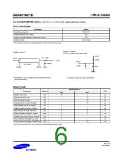
TEST CONDITIONS*
Parameter
Value
Input Pulse Levels
0V to 3V
3ns
Input Rise and Fall Times
Input and Output timing Reference Levels
Output Loads
1.5V
See below
* The above test conditions are also applied at industrial temperature range.
Output Loads(B)
for tHZ, tLZ, tWHZ, tOW, tOLZ & tOHZ
Output Loads(A)
+5.0V
RL = 50W
DOUT
480W
VL = 1.5V
DOUT
30pF*
ZO = 50W
255W
5pF*
* Capacitive Load consists of all components of the
test environment.
* Including Scope and Jig Capacitance
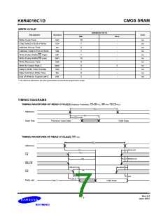
READ CYCLE*
K6R4016C1D-10
Parameter
Symbol
Unit
Min
10
-
Max
Read Cycle Time
tRC
tAA
-
10
10
5
ns
ns
ns
ns
ns
ns
ns
ns
ns
ns
ns
Address Access Time
Chip Select to Output
tCO
tOE
tLZ
-
Output Enable to Valid Output
Chip Enable to Low-Z Output
Output Enable to Low-Z Output
Chip Disable to High-Z Output
Output Disable to High-Z Output
Output Hold from Address Change
Chip Selection to Power Up Time
Chip Selection to Power DownTime
-
3
-
tOLZ
tHZ
tOHZ
tOH
tPU
0
-
0
5
0
5
3
-
0
-
tPD
-
10
* The above parameters are also guaranteed at industrial temperature range.
Rev 2.0
June 2003
- 6 -

 SAMSUNG [ SAMSUNG ]