PRELIMPreliminaryPPPPPPPPPINARY
CMOS SRAM
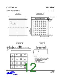
K6R4016C1D
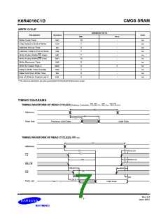
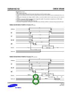
NOTES(READ CYCLE)
1. WE is high for read cycle.
2. All read cycle timing is referenced from the last valid address to the first transition address.
3. tHZ and tOHZ are defined as the time at which the outputs achieve the open circuit condition and are not referenced to VOH or VOL
levels.
4. At any given temperature and voltage condition, tHZ(Max.) is less than tLZ (Min.) both for a given device and from device to
device.
5. Transition is measured ±200mV from steady state voltage with Load(B). This parameter is sampled and not 100% tested.
6. Device is continuously selected with CS=VIL.
7. Address valid prior to coincident with CS transition low.
8. For common I/O applications, minimization or elimination of bus contention conditions is necessary during read and write cycle.
TIMING WAVEFORM OF WRITE CYCLE(1) (OEClock)
tWC
Address
tAW
tWR(5)
OE
tCW(3)
CS
tBW
UB, LB
tAS(4)
tWP(2)
WE
tDW
tDH
High-Z
High-Z
Data in
Data out
Valid Data
tOHZ(6)
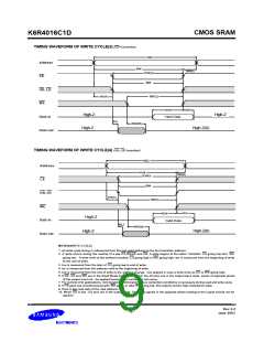
TIMING WAVEFORM OF WRITE CYCLE(2) (OE=Low fixed)
tWC
Address
tAW
tWR(5)
tCW(3)
tBW
CS
UB, LB
tWP1(2)
tAS(4)
WE
tDW
tDH
High-Z
Valid Data
Data in
(9)
(10)
tWHZ(6)
tOW
High-Z
Data out
Rev 2.0
June 2003
- 8 -

 SAMSUNG [ SAMSUNG ]