PRELIMPreliminaryPPPPPPPPPINARY
CMOS SRAM
K6R4016C1D
256K x 16 Bit High-Speed CMOS Static RAM
FEATURES
GENERAL DESCRIPTION
• Fast Access Time 10ns(Max.)
• Low Power Dissipation
Standby (TTL) : 20mA(Max.)
The K6R4016C1D is a 4,194,304-bit high-speed Static Ran-
dom Access Memory organized as 262,144 words by 16 bits.
The K6R4016C1D uses 16 common input and output lines and
has an output enable pin which operates faster than address
access time at read cycle. Also it allows that lower and upper
byte access by data byte control(UB, LB). The device is fabri-
cated using SAMSUNG¢s advanced CMOS process and
designed for high-speed circuit technology. It is particularly well
suited for use in high-density high-speed system applications.
The K6R4016C1D is packaged in a 400mil 44-pin plastic SOJ
or TSOP(II) forward or 48 T BGA.
(CMOS) : 5mA(Max.)
Operating K6R4016C1D-10 : 65mA(Max.)
• Single 5.0V±10% Power Supply
• TTL Compatible Inputs and Outputs
• Fully Static Operation
- No Clock or Refresh required
• Three State Outputs
• Center Power/Ground Pin Configuration
• Data Byte Control : LB : I/O1~ I/O8, UB : I/O9~ I/O16
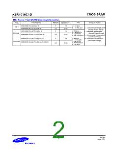
• Standard Pin Configuration
K6R4016C1D-J : 44-SOJ-400
K6R4016C1D-K : 44-SOJ-400(Lead-Free)
K6R4016C1D-T : 44-TSOP2-400BF
K6R4016C1D-U : 44-TSOP2-400BF (Lead-Free)
K6R4016C1D-E : 48-TBGA with 0.75 Ball pitch
(7mm X 9mm)
• Operating in Commercial and Industrial Temperature range.
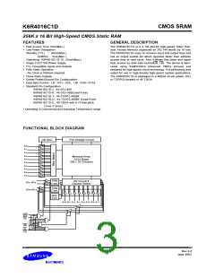
FUNCTIONAL BLOCK DIAGRAM
Clk Gen.
Pre-Charge Circuit
A0
A1
A2
A3
A4
A5
A6
A7
A8
A9
Memory Array
1024 Rows
256 x 16 Columns
Data
Cont.
I/O Circuit &
Column Select
I/O1~I/O 8
Data
Cont.
I/O9~I/O 16
Gen.
CLK
A10 A11 A12 A13 A14 A15 A16 A17
WE
OE
UB
LB
CS
Rev 2.0
June 2003
- 3 -

 SAMSUNG [ SAMSUNG ]