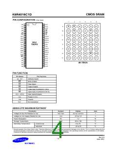
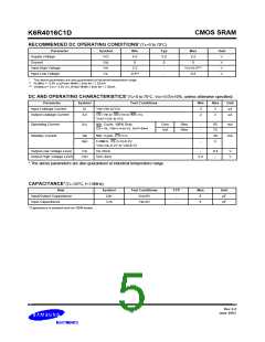
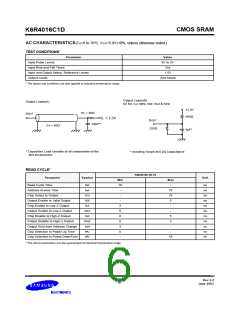
PRELIMPreliminaryPPPPPPPPPINARY
CMOS SRAM
K6R4016C1D
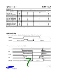
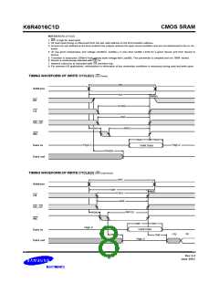
TIMING WAVEFORM OF WRITE CYCLE(3) (CS=Controlled)
tWC
Address
CS
tAW
tWR(5)
tCW(3)
tBW
UB, LB
tAS(4)
WE
tWP(2)
tDW
tDH
High-Z
High-Z
Data in
Valid Data
tLZ
tWHZ(6)
High-Z
High-Z(8)
Data out
TIMING WAVEFORM OF WRITE CYCLE(4) (UB, LBControlled)
tWC
Address
CS
tAW
tCW(3)
tWR(5)
tBW
UB, LB
tAS(4)
tWP(2)
WE
tDH
tDW
High-Z
Data in
Valid Data
tBLZ
tWHZ(6)
High-Z(8)
High-Z
Data out
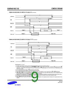
NOTES(WRITE CYCLE)
1. All write cycle timing is referenced from the last valid address to the first transition address.
2. A write occurs during the overlap of a low CS,WE,LB and UB. A write begins at the latest transition CS going low and WE
going low ; A write ends at the earliest transition CS going high or WE going high. tWP is measured from the beginning of write
to the end of write.
3. tCW is measured from the later of CS going low to end of write.
4. tAS is measured from the address valid to the beginning of write.
5. tWR is measured from the end of write to the address change. tWR applied in case a write ends as CS or WE going high.
6. If OE, CS and WE are in the Read Mode during this period, the I/O pins are in the output low-Z state. Inputs of opposite phase
of the output must not . be applied because bus contention can occur.
7. For common I/O applications, minimization or elimination of bus contention conditions is necessary during read and write cycle.
8. If CS goes low simultaneously with WE going or after WE going low, the outputs remain high impedance state.
9. Dout is the read data of the new address.
10. When CS is low : I/O pins are in the output state. The input signals in the opposite phase leading to the output should not be
applied.
Rev 2.0
June 2003
- 9 -

 SAMSUNG [ SAMSUNG ]