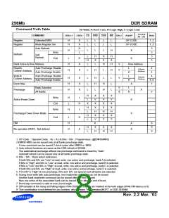
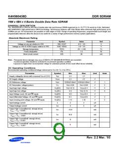
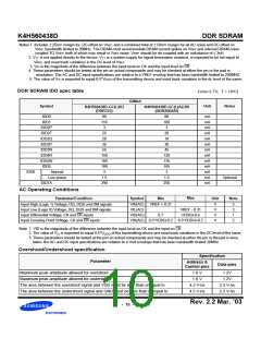
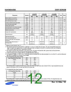
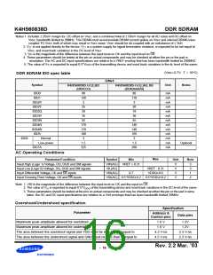
K4H560438D
DDR SDRAM
-GC(L)B3
(DDR333)
-GC(L)A2
(DDR266A)
-GC(L)B0
(DDR266B)
Parameter
Symbol
Unit Note
Min
Max
Min
Max
Min Max
Mode register set cycle time
DQ & DM setup time to DQS
DQ & DM hold time to DQS
tMRD
tDS
12
15
15
ns
0.45
0.5
0.5
ns
ns
7,8,9
7,8,9
tDH
0.45
0.5
0.5
Control & Address input pulse width
DQ & DM input pulse width
Power down exit time
tIPW
2.2
1.75
6
2.2
1.75
7.5
2.2
1.75
7.5
ns
ns
tDIPW
tPDEX
tXSNR
tXSRD
tREFI
ns
Exit self refresh to non-Read command
Exit self refresh to read command
Refresh interval time
75
75
75
ns
4
200
7.8
200
7.8
200
7.8
tCK
us
1
5
tHP
-tQHS
tHP
-tQHS
tHP
-tQHS
Output DQS valid window
Clock half period
tQH
tHP
-
-
-
-
-
-
ns
ns
tCLmin
or tCHmin
tCLmin
or tCHmin
tCLmin
or tCHmin
Data hold skew factor
tQHS
0.5
0.6
0.75
0.6
0.75
0.6
ns
DQS write postamble time
tWPST
0.4
18
0.4
20
0.4
20
tCK
3
Active to Read with Auto precharge
command
tRAP
Autoprecharge write recovery +
Precharge time
(tWR/tCK)
+
(tWR/tCK)
+
(tWR/tCK)
+
tDAL
tCK
11
(tRP/tCK)
(tRP/tCK)
(tRP/tCK)
1. Maximum burst refresh cycle : 8
2. The specific requirement is that DQS be valid(High or Low) on or before this CK edge. The case shown(DQS going from
High_Z to logic Low) applies when no writes were previously in progress on the bus. If a previous write was in progress,
DQS could be High at this time, depending on tDQSS.
3. The maximum limit for this parameter is not a device limit. The device will operate with a great value for this parameter,
but system performance (bus turnaround) will degrade accordingly.
4. A write command can be applied with tRCD satisfied after this command.
5. For registered DIMMs, tCL and tCH are ≥ 45% of the period including both the half period jitter (tJIT(HP)) of the PLL and the half period
jitter due to crosstalk (tJIT(crosstalk)) on the DIMM.
6. Input Setup/Hold Slew Rate Derating
Input Setup/Hold Slew Rate
∆tIS
(ps)
0
∆tIH
(ps)
0
(V/ns)
0.5
0.4
+50
+100
+50
+100
0.3
This derating table is used to increase t /t in the case where the input slew rate is below 0.5V/ns. Input setup/hold slew rate
IS IH
based on the lesser of AC-AC slew rate and DC-DC slew rate.
7. I/O Setup/Hold Slew Rate Derating
I/O Setup/Hold Slew Rate
∆tDS
(ps)
0
∆tDH
(ps)
0
(V/ns)
0.5
0.4
+75
+150
+75
+150
0.3
This derating table is used to increase t /t in the case where the I/O slew rate is below 0.5V/ns. I/O setup/hold slew rate
DS DH
based on the lesser of AC-AC slew rate and DC-DC slew rate.
Rev. 2.2 Mar. ’03
- 12 -

 SAMSUNG [ SAMSUNG ]