K4H560438D
DDR SDRAM
16M x 4Bit x 4 Banks Double Data Rate SDRAM
GENERAL DESCRIPTION
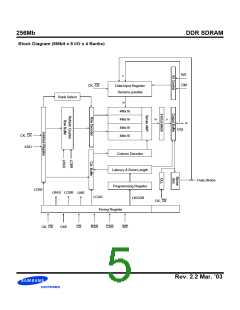
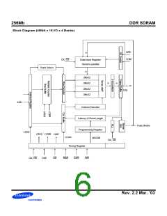
The K4H560438D is 268,435,456 bits of double data rate synchronous DRAM organized as 4 x 16,777,216 words by 4 bits, fabricated
with SAMSUNG′s high performance CMOS technology. Synchronous features with Data Strobe allow extremely high performance up to
333Mb/s per pin. I/O transactions are possible on both edges of DQS. Range of operating frequencies, programmable burst length and
programmable latencies allow the device to be useful for a variety of high performance memory system applications.
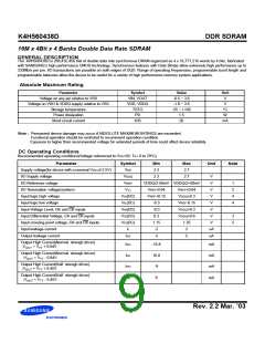
Absolute Maximum Rating
Parameter
Voltage on any pin relative to VSS
Voltage on VDD & VDDQ supply relative to VSS
Storage temperature
Symbol
VIN, VOUT
VDD, VDDQ
TSTG
Value
-0.5 ~ 3.6
-1.0 ~ 3.6
-55 ~ +150
1.5
Unit
V
V
°C
W
Power dissipation
PD
Short circuit current
IOS
50
mA
Note : Permanent device damage may occur if ABSOLUTE MAXIMUM RATINGS are exceeded.
Functional operation should be restricted to recommend operation condition.
Exposure to higher than recommended voltage for extended periods of time could affect device reliability
DC Operating Conditions
Recommended operating conditions(Voltage referenced to VSS=0V, TA= 0 to 70°C)
Parameter
Supply voltage(for device with a nominal VDD of 2.5V)
I/O Supply voltage
Symbol
VDD
Min
2.3
Max
2.7
Unit
Note
VDDQ
VREF
2.3
2.7
V
V
I/O Reference voltage
VDDQ/2-50mV VDDQ/2+50mV
1
2
4
4
I/O Termination voltage(system)
Input logic high voltage
V
VREF-0.04
VREF+0.15
-0.3
VREF+0.04
VDDQ+0.3
VREF-0.15
VDDQ+0.3
VDDQ+0.6
1.35
V
TT
VIH(DC)
VIL(DC)
VIN(DC)
VID(DC)
VIX(DC)
II
V
Input logic low voltage
V
Input Voltage Level, CK and CK inputs
Input Differential Voltage, CK and CK inputs
Input crossing point voltage, CK and CK inputs
Input leakage current
-0.3
V
0.3
V
3
5
1.15
V
-2
2
uA
uA
Output leakage current
IOZ
-5
5
Output High Current(Normal strengh driver)
IOH
IOL
IOH
IOL
-16.8
16.8
-9
mA
mA
mA
mA
;V
= V + 0.84V
OUT
TT
Output High Current(Normal strengh driver)
;V = V - 0.84V
OUT
TT
Output High Current(Half strengh driver)
;V = V + 0.45V
OUT
TT
Output High Current(Half strengh driver)
;V = V - 0.45V
9
OUT
TT
Rev. 2.2 Mar. ’03
- 9 -

 SAMSUNG [ SAMSUNG ]