256Mb
DDR SDRAM
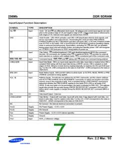
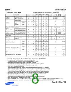
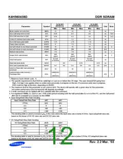
Command Truth Table
(V=Valid, X=Don′t Care, H=Logic High, L=Logic Low)
A11,A12
A9 ~ A0
CKEn-1
CKEn
CS
RAS
CAS
WE
BA0,1
A10/AP
Note
COMMAND
Extended MRS
Register
Register
H
H
X
X
H
L
L
L
L
L
L
L
L
L
OP CODE
OP CODE
1, 2
1, 2
3
Mode Register Set
Auto Refresh
H
L
L
L
H
X
X
Entry
3
Refresh
Self
Refresh
L
H
L
H
X
L
H
X
H
H
X
H
3
Exit
L
H
H
H
X
X
3
Bank Active & Row Address
V
V
Row Address
L
Read &
Auto Precharge Disable
Auto Precharge Enable
Auto Precharge Disable
Auto Precharge Enable
4
4
Column
L
H
L
H
Column Address
Address
H
L
Write &
4
Column
Address
H
H
H
X
X
X
L
L
L
H
H
L
L
H
H
L
L
L
V
Column Address
H
4, 6
7
Burst Stop
Precharge
X
Bank Selection
All Banks
V
X
L
X
H
5
H
L
X
V
X
X
H
X
V
X
X
H
X
V
X
X
H
X
V
X
V
X
X
H
X
V
Entry
Exit
H
L
L
H
L
Active Power Down
X
X
X
H
L
Entry
H
Precharge Power Down Mode
H
L
Exit
L
H
H
H
X
DM
X
X
8
9
9
H
L
X
H
X
H
No operation (NOP) : Not defined
1. OP Code : Operand Code. A0 ~ A12 & BA0 ~ BA1 : Program keys. (@EMRS/MRS)
2.EMRS/ MRS can be issued only at all banks precharge state.
A new command can be issued 2 clock cycles after EMRS or MRS.
3. Auto refresh functions are same as the CBR refresh of DRAM.
The automatical precharge without row precharge command is meant by "Auto".
Auto/self refresh can be issued only at all banks precharge state.
4. BA0 ~ BA1 : Bank select addresses.
If both BA0 and BA1 are "Low" at read, write, row active and precharge, bank A is selected.
If BA0 is "High" and BA1 is "Low" at read, write, row active and precharge, bank B is selected.
If BA0 is "Low" and BA1 is "High" at read, write, row active and precharge, bank C is selected.
If both BA0 and BA1 are "High" at read, write, row active and precharge, bank D is selected.
5. If A10/AP is "High" at row precharge, BA0 and BA1 are ignored and all banks are selected.
6. During burst write with auto precharge, new read/write command can not be issued.
Another bank read/write command can be issued after the end of burst.
New row active of the associated bank can be issued at tRP after the end of burst.
7. Burst stop command is valid at every burst length.
8. DM sampled at the rising and falling edges of the DQS and Data-in are masked at the both edges (Write DM latency is 0).
9. This combination is not defined for any function, which means "No Operation(NOP)" in DDR SDRAM.
Rev. 2.2 Mar. ’03
- 8 -

 SAMSUNG [ SAMSUNG ]