K4H560438D
DDR SDRAM
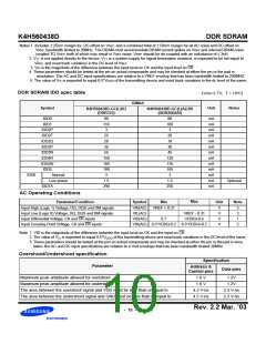
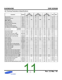
AC Timming Parameters & Specifications
B3
(DDR333)
A2
B0
(DDR266B)
(DDR266A)
Parameter
Symbol
Unit
Note
Min
Max
Min
Max
Min
Max
Row cycle time
tRC
tRFC
tRAS
tRCD
tRP
60
72
65
75
65
75
ns
ns
Refresh row cycle time
Row active time
42
70K
45
120K
45
120K
ns
RAS to CAS delay
18
20
20
ns
Row precharge time
18
20
20
ns
Row active to Row active delay
Write recovery time
tRRD
tWR
12
15
15
ns
15
15
15
ns
Last data in to Read command
Col. address to Col. address delay
tWTR
tCCD
1
1
1
tCK
tCK
ns
1
1
1
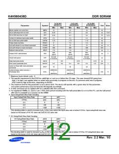
CL=2.0
CL=2.5
7.5
6
12
12
7.5
7.5
0.45
0.45
-0.75
-0.75
-
12
12
10
12
12
5
5
Clock cycle time
tCK
7.5
0.45
0.45
-0.75
-0.75
-
ns
Clock high level width
tCH
tCL
0.45
0.45
-0.6
-0.7
-
0.55
0.55
+0.6
+0.7
0.4
0.55
0.55
+0.75
+0.75
0.5
0.55
0.55
+0.75
+0.75
0.5
tCK
tCK
ns
Clock low level width
DQS-out access time from CK/CK
tDQSCK
tAC
Output data access time from CK/CK
Data strobe edge to ouput data edge
Read Preamble
ns
tDQSQ
tRPRE
tRPST
tDQSS
tWPRES
tWPRE
tDSS
tDSH
tDQSH
tDQSL
tDSC
tIS
ns
5
2
0.9
0.4
0.75
0
1.1
0.9
0.4
0.75
0
1.1
0.9
0.4
0.75
0
1.1
tCK
tCK
tCK
ns
Read Postamble
0.6
0.6
0.6
CK to valid DQS-in
1.25
1.25
1.25
DQS-in setup time
DQS-in hold time
0.25
0.2
0.2
0.35
0.35
0.9
0.75
0.75
0.8
0.8
-0.7
-0.7
0.5
0.5
1.0
0.67
0.25
0.2
0.2
0.35
0.35
0.9
0.9
0.9
1.0
1.0
-0.75
-0.75
0.5
0.5
1.0
0.67
0.25
0.2
0.2
0.35
0.35
0.9
0.9
0.9
1.0
1.0
-0.75
-0.75
0.5
0.5
1.0
0.67
tCK
tCK
tCK
tCK
tCK
tCK
ns
DQS falling edge to CK rising-setup time
DQS falling edge from CK rising-hold time
DQS-in high level width
DQS-in low level width
DQS-in cycle time
1.1
1.1
1.1
Address and Control Input setup time(fast)
Address and Control Input hold time(fast)
Address and Control Input setup time(slow)
Address and Control Input hold time(slow)
Data-out high impedence time from CK/CK
Data-out low impedence time from CK/CK
Input Slew Rate(for input only pins)
Input Slew Rate(for I/O pins)
Output Slew Rate(x4,x8)
6
6
6
6
tIH
ns
tIS
ns
tIH
ns
tHZ
+0.7
+0.7
+0.75
+0.75
+0.75
+0.75
ns
tLZ
ns
tSL(I)
tSL(IO)
tSL(O)
V/ns
V/ns
V/ns
6
7
4.5
1.5
4.5
1.5
4.5
1.5
10
Output Slew Rate Matching Ratio(rise to fall) tSLMR
Rev. 2.2 Mar. ’03
- 11 -

 SAMSUNG [ SAMSUNG ]