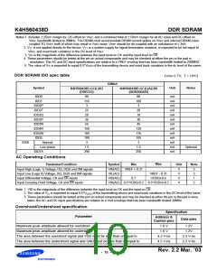
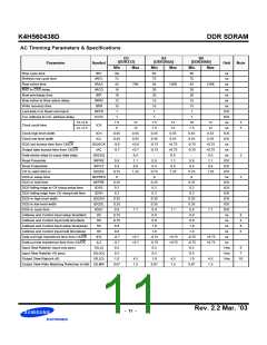
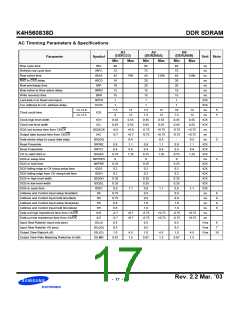
K4H560438D
DDR SDRAM
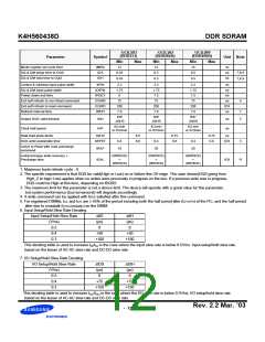
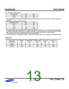
8. I/O Setup/Hold Plateau Derating
I/O Input Level
(mV)
∆tDS
(ps)
∆tDH
(ps)
± 280
+50
+50
This derating table is used to increase tDS/tDH in the case where the input level is flat below VREF ± 310mV for a duration of
up to 2ns.
9. I/O Delta Rise/Fall Rate(1/slew-rate) Derating
Delta Rise/Fall Rate
∆tDS
(ps)
0
∆tDH
(ps)
0
(ns/V)
0
±0.25
±0.5
+50
+100
+50
+100
This derating table is used to increase tDS/tDH in the case where the DQ and DQS slew rates differ. The Delta Rise/Fall Rate
is calated as 1/SlewRate1-1/SlewRate2. For example, if slew rate 1 = 5V/ns and slew rate 2 =.4V/ns then the Delta Rise/Fall
Rate =-0/5ns/V. Input S/H slew rate based on larger of AC-AC delta rise/fall rate and DC-DC delta rise/fall rate.
10. This parameter is fir system simulation purpose. It is guranteed by design.
11. For each of the terms, if not already an integer, round to the next highest integer. tCK is actual to the system clock cycle time.
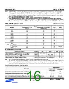
<Reference>
The following table specifies derating values for the specifications listed if the single-ended clock skew rate is less than 1.0V/ns.
CK slew rate
∆tIH/tIS
∆tDSS/tDSH
∆tAC/tDQSCK
∆tLZ(min)
∆tHZ(max)
(Single ended)
(ps)
(ps)
(ps)
(ps)
(ps)
1.0V/ns
0.75V/ns
0.5V/ns
0
0
0
0
0
+50
+100
+50
+100
+50
+100
-50
-100
+50
+100
Rev. 2.2 Mar. ’03
- 13 -

 SAMSUNG [ SAMSUNG ]