K4F170411C, K4F160411C
K4F170412C, K4F160412C
CMOS DRAM
( Note 11 )
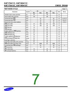
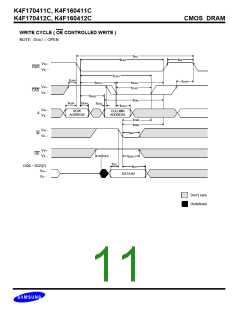
TEST MODE CYCLE
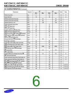
-50
-60
Parameter
Symbol
Units
Notes
Min
95
Max
Min
115
160
Max
Random read or write cycle time
ns
tRC
Read-modify-write cycle time
Access time from RAS
Access time from CAS
Access time from column address
RAS pulse width
138
ns
ns
ns
ns
ns
ns
ns
ns
ns
ns
ns
ns
ns
ns
ns
ns
ns
ns
ns
ns
tRWC
tRAC
tCAC
tAA
55
18
65
20
3,4,10,12
3,4,5,12
3,10,12
30
35
55
18
18
55
30
41
78
53
58
40
81
55
10K
10K
65
20
20
65
35
45
90
60
65
45
90
65
10K
10K
tRAS
tCAS
tRSH
tCSH
tRAL
CAS pulse width
RAS hold time
CAS hold time
Column address to RAS lead time
CAS to W delay time
7
7
7
tCWD
tRWD
tAWD
tCPWD
tPC
RAS to W delay time
Column address to W delay time
CAS precharge to W delay time
Fast Page cycle time
Fast Page read-modify-write cycle time
RAS pulse width (Fast Page cycle)
Access time from CAS precharge
OE access time
tPRWC
tRASP
tCPA
tOEA
tOED
tOEH
200K
35
200K
40
3
18
20
OE to data delay
18
18
20
20
OE command hold time

 SAMSUNG [ SAMSUNG ]