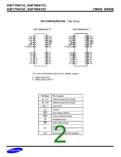
K4F170411C, K4F160411C
K4F170412C, K4F160412C
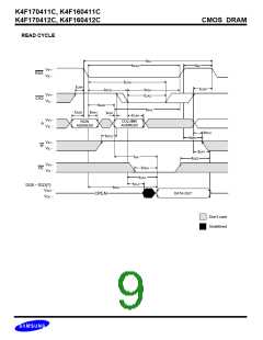
CMOS DRAM
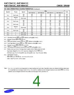
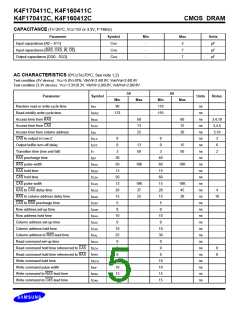
CAPACITANCE (TA=25°C, VCC=5V or 3.3V, f=1MHz)
Parameter
Input capacitance [A0 ~ A11]
Symbol
Min
Max
Units
pF
CIN1
CIN2
CDQ
-
-
-
5
7
7
Input capacitance [RAS, CAS, W, OE]
Output capacitance [DQ0 - DQ3]
pF
pF
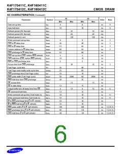
AC CHARACTERISTICS (0°C£TA£70°C, See note 1,2)
Test condition (5V device) : VCC=5.0V±10%, Vih/Vil=2.4/0.8V, Voh/Vol=2.4/0.4V
Test condition (3.3V device) : VCC=3.3V±0.3V, Vih/Vil=2.0/0.8V, Voh/Vol=2.0/0.8V
-50
-60
Parameter
Symbol
Units
Notes
Min
90
Max
Min
110
155
Max
Random read or write cycle time
Read-modify-write cycle time
Access time from RAS
ns
ns
ns
ns
ns
ns
ns
ns
ns
ns
ns
ns
ns
ns
ns
ns
ns
ns
ns
ns
ns
ns
ns
ns
ns
ns
ns
ns
tRC
133
tRWC
tRAC
tCAC
tAA
50
13
25
60
15
30
3,4,10
3,4,5
3,10
3
Access time from CAS
Access time from column address
CAS to output in Low-Z
0
0
0
tCLZ
tOFF
tT
Output buffer turn-off delay
Transition time (rise and fall)
RAS precharge time
0
13
50
15
50
6
3
3
2
30
50
13
50
13
20
15
5
40
60
15
60
15
20
15
5
tRP
RAS pulse width
10K
10K
tRAS
tRSH
tCSH
tCAS
tRCD
tRAD
tCRP
tASR
tRAH
tASC
tCAH
tRAL
tRCS
tRCH
tRRH
tWCH
tWP
RAS hold time
CAS hold time
CAS pulse width
10K
37
10K
45
RAS to CAS delay time
4
RAS to column address delay time
CAS to RAS precharge time
Row address set-up time
Row address hold time
25
30
10
0
0
10
0
10
0
Column address set-up time
Column address hold time
Column address to RAS lead time
Read command set-up time
Read command hold time referenced to CAS
Read command hold time referenced to RAS
Write command hold time
Write command pulse width
Write command to RAS lead time
Write command to CAS lead time
10
25
0
10
30
0
0
0
8
8
0
0
10
10
13
13
10
10
15
15
tRWL
tCWL

 SAMSUNG [ SAMSUNG ]