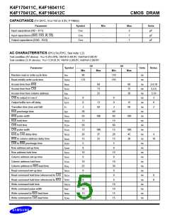
K4F170411C, K4F160411C
K4F170412C, K4F160412C
CMOS DRAM
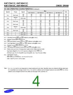
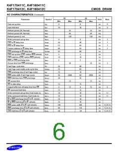
DC AND OPERATING CHARACTERISTICS (Continued)
Max
Symbol
Power
Speed
Units
K4F170412C
K4F160412C
K4F170411C
K4F160411C
-50
-60
90
80
110
100
90
80
110
100
mA
mA
ICC1
ICC2
ICC3
ICC4
ICC5
ICC6
Don¢t care
Normal
L
1
1
1
1
2
1
2
1
mA
mA
Don¢t care
-50
-60
90
80
110
100
90
80
110
100
mA
mA
Don¢t care
Don¢t care
-50
-60
80
70
90
80
80
70
90
80
mA
mA
Normal
L
0.5
200
0.5
200
1
250
1
250
mA
uA
Don¢t care
-50
-60
90
80
110
100
90
80
110
100
mA
mA
Don¢t care
ICC7
ICCS
L
L
Don¢t care
Don¢t care
250
200
250
200
300
250
300
250
uA
uA
ICC1* : Operating Current (RAS and CAS, Address cycling @tRC=min.)
ICC2 : Standby Current (RAS=CAS=W=VIH)
ICC3* : RAS-only Refresh Current (CAS=VIH, RAS, Address cycling @tRC=min.)
ICC4* : Fast Page Mode Current (RAS=VIL, CAS, Address cycling @tPC=min.)
ICC5 : Standby Current (RAS=CAS=W=VCC-0.2V)
ICC6* : CAS-Before-RAS Refresh Current (RAS and CAS cycling @tRC=min.)
ICC7 : Battery back-up current, Average power supply current, Battery back-up mode
Input high voltage(VIH)=VCC-0.2V, Input low voltage(VIL)=0.2V, CAS=0.2V,
DQ=Don¢t care, TRC=31.25us(4K/L-ver), 62.5us(2K/L-ver), TRAS=TRASmin~300ns
ICCS : Self Refresh Current
RAS=CAS=0.2V, W=OE=A0 ~ A11=VCC-0.2V or 0.2V,
DQ0 ~ DQ3=VCC-0.2V, 0.2V or Open
*Note :
ICC1, ICC3, ICC4 and ICC6 are dependent on output loading and cycle rates. Specified values are obtained with the output open.
ICC is specified as an average current. In ICC1, ICC3 and ICC6 address can be changed maximum once while RAS=VIL. In ICC4,
address can be changed maximum once within one fast page mode cycle time, tPC.

 SAMSUNG [ SAMSUNG ]