64M DDR SDRAM
K4D623238B-GC
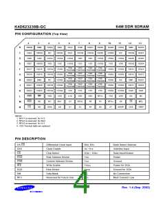
INPUT/OUTPUT FUNCTIONAL DESCRIPTION
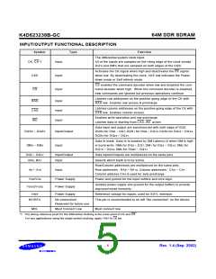
Symbol
Type
Function
The differential system clock Input.
CK, CK*1
Input
Input
Input
All of the inputs are sampled on the rising edge of the clock except
DQ’s and DM’s that are sampled on both edges of the DQS.
Activates the CK signal when high and deactivates the CK signal
when low. By deactivating the clock, CKE low indicates the Power
down mode or Self refresh mode.
CKE
CS
CS enables the command decoder when low and disabled the com-
mand decoder when high. When the command decoder is disabled,
new commands are ignored but previous operations continue.
Latches row addresses on the positive going edge of the CK with
RAS low. Enables row access & precharge.
RAS
CAS
WE
Input
Input
Input
Latches column addresses on the positive going edge of the CK with
CAS low. Enables column access.
Enables write operation and row precharge.
Latches data in starting from CAS, WE active.
Data input and output are synchronized with both edge of DQS.
DQS0 for DQ0 ~ DQ7, DQS1 for DQ8 ~ DQ15, DQS2 for DQ16 ~ DQ23,
DQS3 for DQ24 ~ DQ31.
DQS0 ~ DQS3
DM0 ~ DM3
Input/Output
Input
Data In mask. Data In is masked by DM Latency=0 when DM is high
in burst write. DM0 for DQ0 ~ DQ7, DM1 for DQ8 ~ DQ15, DM2 for
DQ16 ~ DQ23, DM3 for DQ24 ~ DQ31.
DQ0 ~ DQ31
BA0, BA1
Input/Output
Input
Data inputs/Outputs are multiplexed on the same pins.
Selects which bank is to be active.
Row/Column addresses are multiplexed on the same pins.
Row addresses : RA0 ~ RA10, Column addresses : CA0 ~ CA7.
Column address CA8 is used for auto precharge.
A0 ~ A10
Input
VDD/VSS
Power Supply
Power Supply
Power Supply
Power and ground for the input buffers and core logic.
Isolated power supply and ground for the output buffers to provide
improved noise immunity.
VDDQ/VSSQ
VREF
Reference voltage for inputs, used for SSTL interface.
NC/RFU
No connection/
This pin is recommended to be left "No connection" on the device
Reserved for future use
MCL
Must Connect Low
Must connect low
*1 : The timing reference point for the differential clocking is the cross point of CK and CK.
For any applications using the single ended clocking, apply VREF to CK pin.
- 5 -
Rev. 1.4 (Sep. 2002)

 SAMSUNG [ SAMSUNG ]