Rev. 1.01
K4B2G0446D
K4B2G0846D
datasheet
DDR3L SDRAM
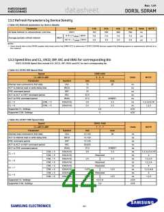
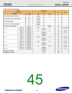
13.2 Refresh Parameters by Device Density
[ Table 44 ] Refresh parameters by device density
Parameter
All Bank Refresh to active/refresh cmd time
Symbol
tRFC
1Gb
110
7.8
2Gb
160
7.8
4Gb
300
7.8
8Gb
350
7.8
Units
ns
NOTE
0 °C ≤ TCASE ≤ 85°C
µs
Average periodic refresh interval
tREFI
85 °C < TCASE ≤ 95°C
3.9
3.9
3.9
3.9
µs
1
NOTE :
1. Users should refer to the DRAM supplier data sheet and/or the DIMM SPD to determine if DDR3 SDRAM devices support the following options or requirements referred to in
this material.
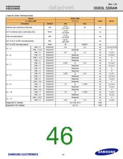
13.3 Speed Bins and CL, tRCD, tRP, tRC and tRAS for corresponding Bin
DDR3 SDRAM Speed Bins include tCK, tRCD, tRP, tRAS and tRC for each corresponding bin.
[ Table 45 ] DDR3-800 Speed Bins
Speed
CL-nRCD-nRP
DDR3-800
6 - 6 - 6
Units
NOTE
Parameter
Symbol
tAA
min
15
max
20
Internal read command to first data
ACT to internal read or write delay time
PRE command period
ns
ns
tRCD
15
-
tRP
15
-
-
ns
ACT to ACT or REF command period
ACT to PRE command period
tRC
52.5
37.5
3.0
2.5
ns
tRAS
9*tREFI
3.3
ns
CL = 5
CWL = 5
CWL = 5
tCK(AVG)
tCK(AVG)
ns
1,2,3,4,9,10
1,2,3
CL = 6
3.3
ns
Supported CL Settings
Supported CWL Settings
5,6
5
nCK
nCK
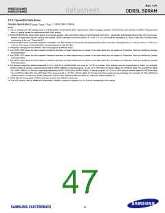
[ Table 46 ] DDR3-1066 Speed Bins
Speed
DDR3-1066
7 - 7 - 7
CL-nRCD-nRP
Units
NOTE
Parameter
Internal read command to first data
ACT to internal read or write delay time
PRE command period
Symbol
tAA
min
13.125
13.125
13.125
50.625
37.5
max
20
ns
ns
tRCD
-
tRP
-
-
ns
ACT to ACT or REF command period
ACT to PRE command period
tRC
ns
tRAS
9*tREFI
3.3
ns
CWL = 5
CWL = 6
CWL = 5
CWL = 6
CWL = 5
CWL = 6
CWL = 5
CWL = 6
tCK(AVG)
tCK(AVG)
tCK(AVG)
tCK(AVG)
tCK(AVG)
tCK(AVG)
tCK(AVG)
tCK(AVG)
3.0
ns
1,2,3,4,5,9,10
CL = 5
CL = 6
CL = 7
CL = 8
Reserved
ns
4
1,2,3,5
1,2,3,4
4
2.5
3.3
ns
Reserved
Reserved
ns
ns
1.875
1.875
<2.5
<2.5
ns
1,2,3,4,8
4
Reserved
ns
ns
1,2,3
Supported CL Settings
Supported CWL Settings
5,6,7,8
5,6
nCK
nCK
- 44 -

 SAMSUNG [ SAMSUNG ]