Rev. 1.01
K4B2G0446D
K4B2G0846D
datasheet
DDR3L SDRAM
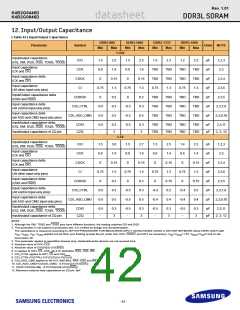
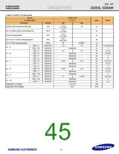
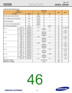
12. Input/Output Capacitance
[ Table 43 ] Input/Output Capacitance
DDR3-800
Min Max
1.35V
DDR3-1066
DDR3-1333
DDR3-1600
Parameter
Symbol
Units NOTE
Min
Max
Min
Max
Min
Max
Input/output capacitance
CIO
CCK
1.5
0.8
0
2.5
1.6
0.15
1.3
0.2
0.3
0.5
1.5
0.8
0
2.5
1.6
0.15
1.3
0.2
0.3
0.5
1.5
2.3
1.2
2.3
TBD
TBD
1.3
pF
pF
pF
pF
pF
pF
pF
1,2,3
2,3
(DQ, DM, DQS, DQS, TDQS, TDQS)
Input capacitance
(CK and CK)
TBD
TBD
0.75
TBD
TBD
TBD
TBD
TBD
1.3
TBD
TBD
0.75
TBD
TBD
TBD
Input capacitance delta
(CK and CK)
CDCK
2,3,4
Input capacitance
(All other input-only pins)
CI
0.75
0
0.75
0
2,3,6
Input/Output capacitance delta
(DQS and DQS)
CDDQS
CDI_CTRL
CDI_ADD_CMD
TBD
TBD
TBD
TBD
TBD
TBD
2,3,5
Input capacitance delta
(All control input-only pins)
-0.5
-0.5
-0.5
-0.5
2,3,7,8
2,3,9,10
Input capacitance delta
(all ADD and CMD input-only pins)
Input/output capacitance delta
CDIO
CZQ
-0.5
-
0.3
3
-0.5
-
0.3
3
TBD
TBD
TBD
TBD
TBD
TBD
TBD
TBD
pF
pF
2,3,11
(DQ, DM, DQS, DQS, TDQS, TDQS)
Input/output capacitance of ZQ pin
2, 3, 12
1.5V
Input/output capacitance
CIO
CCK
1.5
0.8
0
3.0
1.6
0.15
1.5
0.2
0.3
0.5
1.5
0.8
0
2.7
1.6
0.15
1.5
0.2
0.3
0.5
1.5
0.8
0
2.5
1.4
1.4
0.8
0
2.3
1.4
pF
pF
pF
pF
pF
pF
pF
1,2,3
2,3
(DQ, DM, DQS, DQS, TDQS, TDQS)
Input capacitance
(CK and CK)
Input capacitance delta
(CK and CK)
CDCK
0.15
1.3
0.15
1.3
2,3,4
Input capacitance
(All other input-only pins)
CI
0.75
0
0.75
0
0.75
0
0.75
0
2,3,6
Input capacitance delta
(DQS and DQS)
CDDQS
CDI_CTRL
CDI_ADD_CMD
0.15
0.2
0.15
0.2
2,3,5
Input capacitance delta
(All control input-only pins)
-0.5
-0.5
-0.5
-0.5
-0.4
-0.4
-0.4
-0.4
2,3,7,8
2,3,9,10
Input capacitance delta
(all ADD and CMD input-only pins)
0.4
0.4
Input/output capacitance delta
CDIO
CZQ
-0.5
-
0.3
3
-0.5
-
0.3
3
-0.5
-
0.3
3
-0.5
-
0.3
3
pF
pF
2,3,11
(DQ, DM, DQS, DQS, TDQS, TDQS)
Input/output capacitance of ZQ pin
2, 3, 12
NOTE :
1. Although the DM, TDQS and TDQS pins have different functions, the loading matches DQ and DQS
2. This parameter is not subject to production test. It is verified by design and characterization.
The capacitance is measured according to JEP147("PROCEDURE FOR MEASURING INPUT CAPACITANCE USING A VECTOR NETWORK ANALYZER( VNA)") with
V
, V
, V , V
applied and all other pins floating (except the pin under test, CKE, RESET and ODT as necessary). V =V
=1.5V, V
=V /2 and on-die
BIAS DD
DD
DDQ
SS
SSQ
DD
DDQ
termination off.
3. This parameter applies to monolithic devices only; stacked/dual-die devices are not covered here
4. Absolute value of CCK-CCK
5. Absolute value of CIO(DQS)-CIO(DQS)
6. CI applies to ODT, CS, CKE, A0-A15, BA0-BA2, RAS, CAS, WE.
7. CDI_CTRL applies to ODT, CS and CKE
8. CDI_CTRL=CI(CTRL)-0.5*(CI(CLK)+CI(CLK))
9. CDI_ADD_CMD applies to A0-A15, BA0-BA2, RAS, CAS and WE
10. CDI_ADD_CMD=CI(ADD_CMD) - 0.5*(CI(CLK)+CI(CLK))
11. CDIO=CIO(DQ,DM) - 0.5*(CIO(DQS)+CIO(DQS))
12. Maximum external load capacitance on ZQ pin: 5pF
- 42 -

 SAMSUNG [ SAMSUNG ]