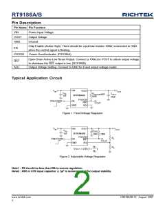
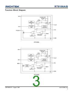
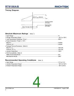
RT9186A/B
Note 1. Stresses listed as the above "Absolute Maximum Ratings" may cause permanent damage to the device. These are for
stress ratings. Functional operation of the device at these or any other conditions beyond those indicated in the
operational sections of the specifications is not implied. Exposure to absolute maximum rating conditions for extended
periods may remain possibility to affect device reliability.
Note 2. Devices are ESD sensitive. Handling precaution is highly recommended.
Note 3. The operating conditions beyond the recommended range is not guaranteed.
Note 4. qJA is measured in the natural convection at TA = 25°C on a low effective thermal conductivity test board (single-layer,
1S) of JEDEC 51-3 thermal measurement standard.
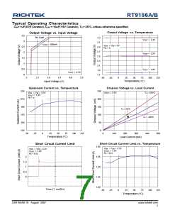
Note 5. The dropout voltage is defined as VIN -VOUT, which is measured when VOUT is VOUT(NORMAL) - 100mV.
Note 6. Quiescent, or ground current, is the difference between input and output currents. It is defined by IQ = IIN - IOUT under
no load condition (IOUT = 0mA). The total current drawn from the supply is the sum of the load current plus the ground
pin current.
Note 7. Regulation is measured at constant junction temperature by using a 20ms current pulse. Devices are tested for load
regulation in the load range from 1mA to 300mA and 500mA respectively.
www.richtek.com
6
DS9186AB-10 August 2007

 RICHTEK [ RICHTEK TECHNOLOGY CORPORATION ]