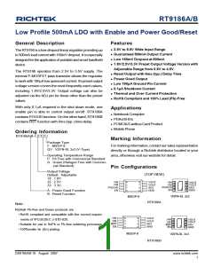
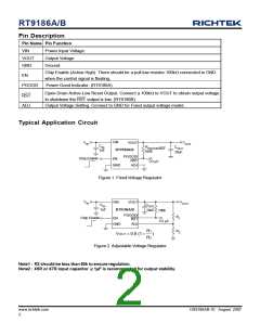
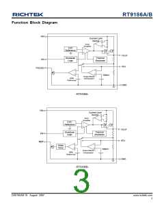
RT9186A/B
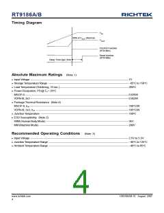
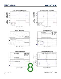
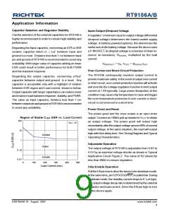
Timing Diagram
V
V
IN
80% of V
(Normal)
OUT
OUT
PGOOD Function
(RT9186A)
Reset function
(RT9186B)
Delay Time (typ.) 6ms
Absolute Maximum Ratings (Note 1)
l Input Voltage ---------------------------------------------------------------------------------------------------------- 7V
l StorageTemperature Range --------------------------------------------------------------------------------------- - 65°C to 150°C
l Lead Temperature (Soldering, 10 sec.)-------------------------------------------------------------------------- 260°C
l PowerDissipation, PD @ TA = 25°C
MSOP-8---------------------------------------------------------------------------------------------------------------- 0.625W
VDFN-8L 3x3---------------------------------------------------------------------------------------------------------- 0.952W
l Package Thermal Resistance (Note 4)
MSOP-8, qJA ---------------------------------------------------------------------------------------------------------- 160°C/W
VDFN-8L 3x3, qJA ---------------------------------------------------------------------------------------------------- 105°C/W
l JunctionTemperature ----------------------------------------------------------------------------------------------- 150°C
l ESD Susceptibility (Note 2)
HBM (Human Body Mode) ----------------------------------------------------------------------------------------- 2kV
MM (Machine Mode) ------------------------------------------------------------------------------------------------ 200V
Recommended Operating Conditions (Note 3)
l Input Voltage ---------------------------------------------------------------------------------------------------------- 2.5V to 5.5V
l Junction Temperature Range -------------------------------------------------------------------------------------- - 40°C to 125°C
l AmbientTemperature Range -------------------------------------------------------------------------------------- - 40°C to 85°C
www.richtek.com
4
DS9186AB-10 August 2007

 RICHTEK [ RICHTEK TECHNOLOGY CORPORATION ]