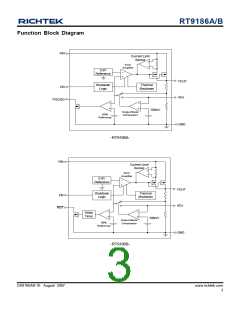
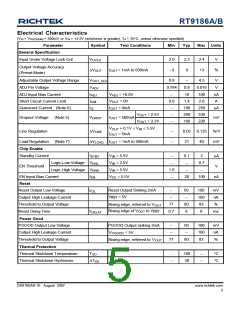
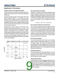
RT9186A/B
Pin Description
Pin Name Pin Function
VIN
Power Input Voltage.
VOUT
GND
Output Voltage.
Ground.
Chip Enable (Active-High). There should be a pull low resistor 100kW connected to GND
EN
when the control signal is floating.
PGOOD
RST
Power Good Indicator. (RT9186A).
Open-Drain Active-Low Reset Output. Connect a 100kW to VOUT to obtain output voltage.
In shutdown the RST output is low. (RT9186B).
ADJ
Output Voltage Setting. Connect to GND for Fixed output voltage model.
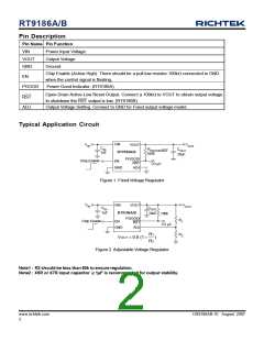
Typical Application Circuit
VIN
V
V
OUT
VOUT
IN
C
1uF
R
100k
C
IN
PGOOD/RST
OUT
RT9186A/B
10uF
PGOOD/
RST
Chip Enable
EN
TO mC
ADJ
GND
Figure 1. FixedVoltage Regulator
V
V
VIN
VOUT
IN
OUT
C
C
OUT
IN
1uF
RT9186A/B
10uF
100k
PGOOD/
RST
R
1
Chip Enable
EN
TO mC
GND
ADJ
R1
)
R2
R
2
VOUT = 0.8 (1+
Figure 2. Adjustable Voltage Regulator
Note1 : R2 should be less than 80k to ensure regulation.
Note2 : X5R or X7R input capacitor ≧1mF is recommended for output stability.
www.richtek.com
2
DS9186AB-10 August 2007

 RICHTEK [ RICHTEK TECHNOLOGY CORPORATION ]