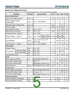
RT9186A/B
Electrical Characteristics
(VIN = VOUT(NOM) + 500mV or VIN = +2.5V (whichever is greater), TA = 25°C, unless otherwise specified)
Parameter
General Specification
Symbol
Test Conditions
= 1mA to 500mA
= +0.8V
Min
Typ
Max Units
Input Under Voltage Lock-Out
V
2.0
- 3
2.3
0
2.4
+3
V
%
V
UVLO
Output Voltage Accuracy
(Preset Mode)
DV
I
OUT
OUT
Adjustable Output Voltage Range
V
V
0.8
--
4.5
OUT_ADJ
ADJ
ADJ Pin Voltage
0.784
--
0.8
10
0.816
100
2.0
V
nA
A
ADJ Input Bias Current
Short Circuit Current Limit
Quiescent Current (Note 6)
I
I
I
V
V
ADJ
ADJ
= 0V
0.9
--
1.4
190
200
160
LIM
Q
OUT
I
= 0mA
250
330
220
mA
OUT
V
V
= 2.5V
= 3.3V
--
OUT
OUT
Dropout Voltage
Line Regulation
(Note 5)
V
I
= 500mA
mV
DROP
OUT
--
V
+ 0.1V < V < 5.5V
IN
OUT
DV
DV
--
0.02 0.125
%/V
mV
LINE
I
= 5mA
OUT
Load Regulation
Chip Enable
(Note 7)
I
= 1mA to 500mA
--
21
40
LOAD
OUT
Standby Current
I
V
V
V
V
= 5.5V
= 2.5V
= 5.5V
= 5.5V
--
--
0.1
--
2
0.7
--
mA
V
STBY
IN
IN
IN
CE
Logic-Low Voltage
Logic-High Voltage
V
V
ENL
ENH
EN Threshold
1.6
--
--
EN Input Bias Current
Reset
I
20
100
nA
EN
Reset Output Low Voltage
Output High Leakage Current
Threshold to Output Voltage
Reset Delay Time
Reset Output Sinking 2mA
= 5V
--
--
50
--
100
100
83
mV
nA
%
V
OL
V
RST
77
0.7
80
6
Rising edge, referred to V
OUT
Rising edge of V
to V
8
ms
OUT
RST
T
DELAY
Power Good
PGOOD Output Low Voltage
Output High Leakage Current
Threshold to Output Voltage
PGOOD Output sinking 2mA
VPGOOD = 5V
--
--
50
--
100
100
83
mV
nA
%
77
80
Rising edge, referred to VOUT
Thermal Protection
Thermal Shutdown Temperature
Thermal Shutdown Hysteresis
T
--
--
160
30
--
--
°C
°C
SD
DT
SD
DS9186AB-10 August 2007
www.richtek.com
5

 RICHTEK [ RICHTEK TECHNOLOGY CORPORATION ]