RT9186A/B
Application Information
Capacitor Selection and Regulator Stability
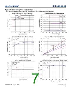
Input-Output (Dropout) Voltage
Careful selection of the external capacitors for RT9186 is
highly recommended in order to remain high stability and
performance.
A regulator’ s minimum input-to-output voltage differential
(dropout voltage) determines the lowest usable supply
voltage. In battery-powered systems, this determines the
useful end-of-life battery voltage. Because the device uses
a P-MOSFET, its dropout voltage is a function of drain-to-
source on-resistance, RDS(ON), multiplied by the load
current:
Regarding the Input capacitor, connecting an X7R or X5R
ceramic capacitor which is ≧1mF between input and
ground is a must. Distance less than 1 cm between input
pin and ground of RT9186 is recommended to avoid any
unstability. With larger value of capacitor adding on lower
ESR could result in better performance for both PSRR
and line transient response.
VDROPOUT = VIN -VOUT = RDS(ON) IOUT
Over-Current and Short-Circuit Protection
The RT9186 continuously monitors output current to
provide maximum safety. Inthe event of output overcurrent
or short-circuit, over-current protection function will activate
and override the voltage regulation function to limit output
current at 1.4A typically. Large power dissipation at this
condition may cause chip temperature to raise and trigger
the over temperature protection if over-current or short-
circuit is not removed in a short time
Regarding the output capacitor, connecting a10mF
capacitor between output and ground is a must. Any
capacitor is acceptable only with a highlight of relation
between ESR region and Load current, shown in below.
Output capacitor with larger capacitance can reduce noise
and improve load transient response, stability, and PSRR.
The same as Input capacitor, distance less than 1 cm
between output pinand ground of RT9186 is recommended
to avoid any unstability.
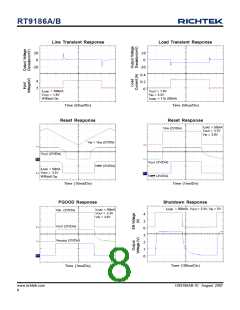
Power Good and Reset
The power good and the reset output is an open-drain
output. Connect an 100kW pull up resistor toVOUT to obtain
an output voltage. The power good will output high
immediately after the output voltage arrives 80% of normal
output voltage. In the same situation, the reset will output
high with 6ms delay time. SeeTimingDiagram andTypical
Operating Characteristics.
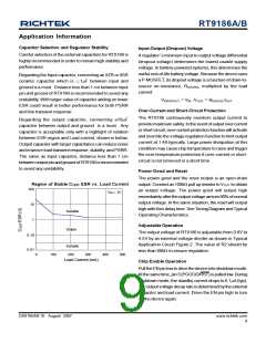
Region of Stable COUT ESR vs. Load Current
100.00
100
VIN = 3V
10.00
10
Instable
Stable
1.00
1
Adjustable Operation
The output voltage of RT9186 is adjustable from 0.8V to
4.5V by an external voltage divider as shown in Typical
Application Circuit Figure 2. The value of R2 should be
less than 80kW to ensure regulation.
0.10
0.10
Instable
200
0.01
0.01
0
100
300
400
500
Load Current (mA)
Chip Enable Operation
Pull the EN pin low to drive the device into shutdown mode.
At the same time, pin 3 (PGOOD/RST) is pulled low.During
shutdown mode, the standby current drops to 0.1mA (typ).
The output voltage decay rate is determined by the external
capacitor and load current. Drive the EN pin high to turn
on the device again.
DS9186AB-10 August 2007
www.richtek.com
9

 RICHTEK [ RICHTEK TECHNOLOGY CORPORATION ]