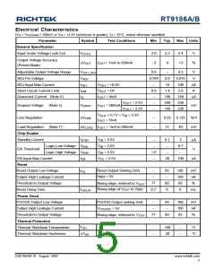
RT9186A/B
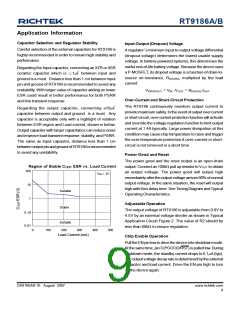
Reverse Current Path
surroundings airflow and temperature difference between
junction to ambient. The maximum power dissipation can
be calculated by following formula :
The P-MOSFET pass element of RT9186 has an
inherendiode connected between the regulator input and
output as shown in Figure 3. The inherent diode will be
forward biased and conduct an unlimited current if VOUT is
PD(MAX) = ( TJ(MAX) - TA ) / qJA
Where TJ(MAX) is the maximum operation junction
temperature 125°C, TA is the ambienttemperature and the
qJA is the junction to ambient thermal resistance.
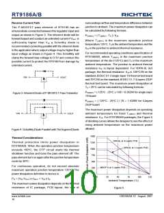
sufficiently higher than VIN a Schottky diode is
.
recommended connecting parallel with the inherent diode
in the application where output voltage may be higher than
input voltage as shown in Figure 4. This Schottkly will
clamp the forward bias voltage to 0.3V and conduct the
possible current to protect the RT9186 from damage by
unlimited current.
For recommended operating conditions specification of
RT9186A/B, where TJ(MAX) is the maximum junction
temperature of the die (125°C) and TA is the maximum
ambient temperature. The junction to ambient thermal
resistance qJA is layout dependent. For VDFN-8L 3x3
package, the thermal resistance qJA is 105°C/W on the
standard JEDEC 51-3 single-layer 1S thermal test board
and 70°C/W on the standard JEDEC 51-7 4-layers 2S2P
thermal test board. The maximum power dissipation at
TA = 25°C can be calculated by following formula :
VIN
VOUT
PD(MAX) = ( 125°C - 25°C ) / 105 = 0.952W for single-layer
Figure 3. InherentDiode of P-MOSFET PassTransistor
1S board
PD(MAX) = ( 125°C - 25°C ) / 70 = 1.428W for 4-layers
2S2P board
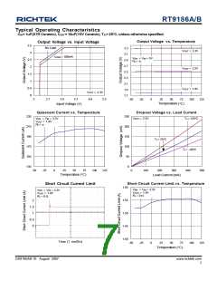
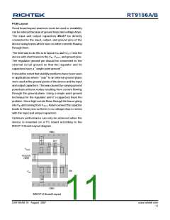
The maximum power dissipation depends on operating
ambient temperature for fixed TJ(MAX) and thermal
resistance qJA. For RT9186A/B packages, the Figure 5
of derating curves allows the designer to see the effect of
rising ambient temperature on the maximum power
allowed.
VIN
VOUT
Figure 4. SchottklyDiode Parallel withThe IngerentDiode
1500
Thermal Considerations
DFN-8L at 4-Layers PCB
1250
Thermal protection limits power dissipation in
RT9186A/B. When the operation junction temperature
exceeds 160°C, the OTP circuit starts the thermal
shutdown function and turns the pass element off. The
pass element turn on again after the junction temperature
cools by 30°C.
DFN-8L at 1-Layers PCB
1000
750
500
For continuous operation, do not exceed absolute
maximum operation junction temperature 125°C. The
power dissipation definition in device is :
MSOP-8 at 1-Layers PCB
250
0
0
25
50
75
100
125
PD = (VIN-VOUT) x IOUT + VIN x IQ
Ambient Temperature (°C)
The maximum power dissipation depends on the thermal
resistance of IC package, PCB layout, the rate of
Figure 5
www.richtek.com
10
DS9186AB-10 August 2007

 RICHTEK [ RICHTEK TECHNOLOGY CORPORATION ]