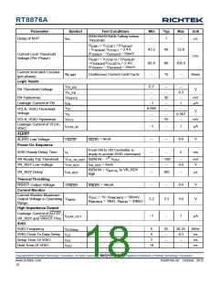
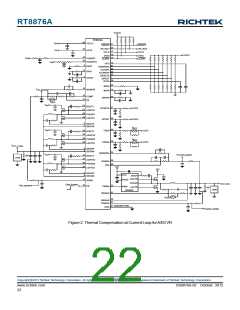
RT8876A
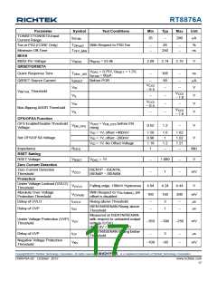
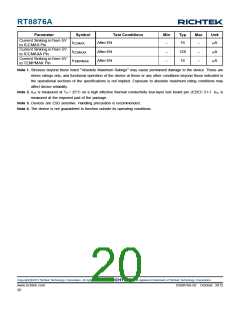
Parameter
Symbol
tNV
Test Conditions
Min
Typ
Max
Unit
ISEN1N/ISENAN Falling below
Threshold
Delay of NVP
--
1
--
μs
GILIMT = VOCSET / (VISENxP
− VISENxN) VOCSET = 2.4V,
(VISENxP − VISENxN) = 50mV
43.2
48
52.8
Current Limit Threshold
Voltage (Per Phase)
V/V
G
ILIMT = VOCSETA / (VISENAP
−VISENAN) VOCSETA = 2.4V,
(VISENAP − VISENAN) = 25mV
86.4
--
96
15
105.6
--
Current limit latch Counter
(per phase)
NILIMIT
Continuous Current Limit Cycle
times
V
Logic Inputs
VIH_EN
VIL_EN
VENHYS
IEN
0.7
--
--
--
--
0.3
--
EN Threshold Voltage
EN Hysteresis
--
30
--
mV
Leakage Current of EN
−1
0.665
--
1
μA
VIH
--
--
VCLK, VDIO Threshold
Voltage
V
VIL
--
0.367
--
VCLK, VDIO Hysteresis
VHYS
--
70
mV
Leakage Current of VCLK,
VDIO
ILEAK_IN
VALERT
tA
−1
--
--
--
--
1
0.4
2
μA
ALERT
IALERT = 4mA
V
ALERT Low Voltage
Power On Sequence
From EN to VR Controller is
ready to accept SVID command
SVID Ready Delay Time
--
ms
VR Ready Trip Threshold
VR_RDY Low Voltage
VTH_VR_RDY ISEN1N − 1st VDAC
--
--
−100
--
mV
V
VVR_RDY
IVR_RDY = 4mA
--
0.4
ISEN1N = VINITIAL to VR_RDY
high
VR_RDY Delay
tVR_RDY
--
100
--
--
μs
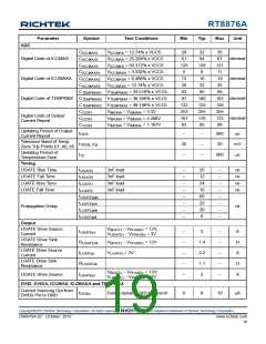
Thermal Throttling
--
0.4
V
VRHOT Output Voltage
Current Monitor
VVRHOT
IVRHOT = 40mA
Current Monitor Maximum
Output Voltage in Operating VIMON
Range
VDAC = 1V, VRIMONFB = 100mV,
RIMONFB = 10kΩ, RIMON = 330kΩ
3.2
3.3
--
3.4
1
V
High Impedance Output
Leakage Current of ALERT,
ILEAK_OUT
−1
μA
VR_RDY and VRHOT Pins
SVID
SVID Frequency
fSVIDfreq
5
4
25
--
26.25
8.3
--
MHz
ns
SVID Clock To Data Delay tCO
Setup Time Of VDIO
Hold Time Of VDIO
tSU
7
--
ns
tHLD
14
--
--
ns
Copyright 2012 Richtek Technology Corporation. All rights reserved.
©
is a registered trademark of Richtek Technology Corporation.
www.richtek.com
18
DS8876A-02 October 2012

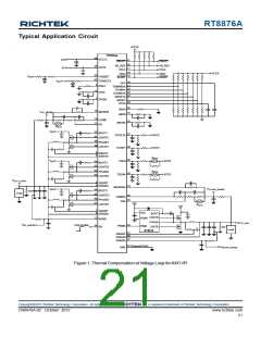
 RICHTEK [ RICHTEK TECHNOLOGY CORPORATION ]