RT8876A
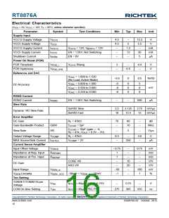
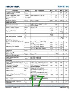
Parameter
Symbol
Test Conditions
Min
Typ
Max
Unit
TONSET/TONSETA Input
Current Range
I
25
--
280
μA
RTON
Ton in PS2 (CORE Only)
Minimum Off-Time
IBIAS
T
T
With Respect to PS0 Ton
--
--
85
--
--
%
ON ps2
250
ns
OFF_MIN
IBIAS Pin Voltage
QRSET/QRSETA
V
R
IBIAS
= 53.6k
2.09
2.14
2.19
V
IBIAS
V
I
= 0.75V, Q
= 80μA
= 1.2V,
RSET
DAC
Quick Response Tonx
QRSET Source Current
T
I
--
--
305
80
--
--
--
--
ns
μA
V
ONx _QR
RTON
Before POR
QRSET
V
CC5
− 0.5
V
IH
IL
IH
IL
V
Threshold
INITIAL
V
CC5
− 1.8
V
V
V
--
--
--
--
V
V
V
V
CC5
− 0.5
--
Non-flipping ADDR Threshold
V
CC5
− 1.8
--
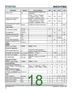
OFS/OFSA Function
OFS Enable/Disable Threshold
Voltage
V
rising
> V
before EN
OFS
EN_OFS
V
0.52
1.2
--
V
EN_OFS
V
V
V
= 1V, offset +400mV
= 1V, offset −200mV
= 1V. No Offset Voltage
1.58
0.98
1.19
1
1.6
1
1.62
1.02
1.21
--
ID
ID
ID
Set OFS/OFSA Voltage
V
MΩ
V
1.2
--
Impedance
R
OFS
RSET Setting
RSET Voltage
V
RSET
V
= 1V
--
--
1.000
1
--
--
DAC
Zero Current Detection
Zero Current Detection
Threshold
ISEN1P − ISEN1N,
ISENAP − ISENAN
V
mV
ZCD
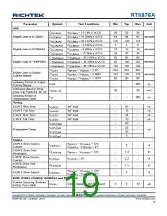
Protection
Under Voltage Lockout (UVLO)
Threshold
V
Falling edge, 100mV Hysteresis
4.04
4.24
4.44
V
UVLO
Absolute Over Voltage
Protection Threshold
With Respect to V
offset is disabled
, pin
OUT(MAX)
V
t
100
--
150
3
200
--
mV
μs
OVABS
Delay of UVLO
Rising above Threshold
UVLO
OV
ISEN1N/ISENAN Rising above
Threshold
Delay of OVP
t
--
1
--
μs
Measured at ISEN1N/ISENAN
with respect to unloaded output
voltage (UOV)
Under Voltage Protection (UVP)
Threshold
V
−350
−300
−250
mV
UV
NV
(for 0.8V < UOV < 1.52V)
ISEN1N/ISENAN Falling below
Threshold
Delay of UVP
t
--
3
--
--
μs
UV
Negative Voltage Protection
Threshold
V
−100
−50
mV
Copyright 2012 Richtek Technology Corporation. All rights reserved.
©
is a registered trademark of Richtek Technology Corporation.
DS8876A-02 October 2012
www.richtek.com
17

 RICHTEK [ RICHTEK TECHNOLOGY CORPORATION ]