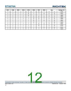
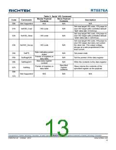
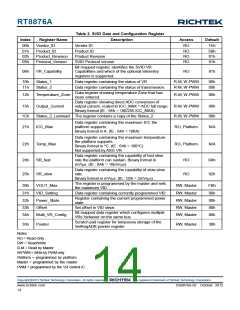
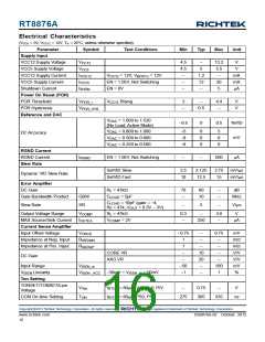
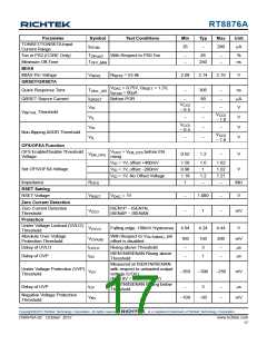
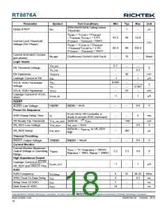
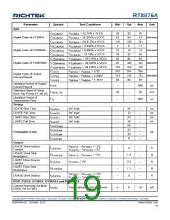
RT8876A
Electrical Characteristics
(VCC5 = 5V, VCC12 = 12V, TA = 25°C, unless otherwise specified)
Parameter
Supply Input
Symbol
Test Conditions
Min
Typ
Max
Unit
VCC12 Supply Voltage
VCC5 Supply Voltage
VCC12 Supply Current
VCC5 Supply Current
Shutdown Current
V
V
4.5
4.5
--
--
5
13.2
5.5
--
V
CC12
CC5
V
I
I
I
V
= 12V, V = 12V
BOOTx
1.2
12
--
mA
mA
μA
VCC12
VCC5
SHDN
CC12
EN = 1.05V, Not Switching
EN = 0V
--
20
5
--
Power On Reset (POR)
POR Threshold
V
V
V
Rising
3
--
4.4
--
V
V
POR_r
CC12
POR Hysteresis
--
0.5
POR_HYS
Reference and DAC
V
= 1.000 to 1.520
DAC
−0.5
0
0.5
%VID
mV
(No Load, Active Mode)
V
V
V
= 0.800 to 1.000
= 0.500 to 0.800
= 0.250 to 0.500
−5
−8
−8
0
0
0
5
8
8
DAC
DAC
DAC
DC Accuracy
RGND Current
RGND Current
Slew Rate
I
EN = 1.05V, Not Switching
--
--
500
μA
RGND
SetVID Slow
SetVID Fast
2.5
10
3.125
12.5
3.75
15
mV/μs
mV/μs
Dynamic VID Slew Rate
Error Amplifier
DC Gain
R = 47kΩ
70
--
80
10
--
--
dB
L
Gain-Bandwidth Product
GBW
SR
C
LOAD
= 5pF
MHz
C
LOAD
= 10pF (gain = −4,
Slew Rate
--
5
--
V/μs
R = 47k, V
F
= 0.5V − 3V)
OUT
Output Voltage Range
MAX Source/Sink Current
Current Sense Amplifier
Input Offset Voltage
V
R = 47kΩ
0.3
--
--
3.6
--
V
COMP
L
I
V
= 2V
COMP
250
μA
OUTEA
V
OSCS
−0.75
1
--
--
0.75
--
mV
mΩ
mΩ
V/V
V/V
mV
%
Impedance at Neg. Input
Impedance at Pos. Input
R
ISENxN
R
1
--
--
ISENxP
CORE VR
AXG VR
--
10
20
--
--
DC Gain
--
--
Input Range
V
−50
−1
100
1
ISEN_in
V
Linearity
V
−30mV < V < 50mV
ISEN_in
--
ISEN
ISEN _ACC
Ton Setting
TONSET/TONSETA pin
Voltage
V
I
I
= 80μA, V = 0.75V
DAC
--
0.75
305
--
V
To n
RTON
RTON
CCM On-time Setting
T
= 80μA, PS0, PS1
275
335
ns
ON
Copyright 2012 Richtek Technology Corporation. All rights reserved.
©
is a registered trademark of Richtek Technology Corporation.
www.richtek.com
16
DS8876A-02 October 2012

 RICHTEK [ RICHTEK TECHNOLOGY CORPORATION ]