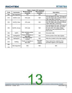
RT8876A
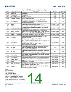
Table 3. SVID Data and Configuration Register
Description
Index
Register Name
Access
Default
00h
01h
02h
05h
Vendor_ID
Vendor ID
RO
RO
RO
RO
1Eh
5Bh
01h
01h
Product_ID
Product ID
Product_Revision
Protocol_Version
Product Revision
SVID Protocol version
Bit mapped register, identifies the SVID VR
Capabilities and which of the optional telemetry
registers is supported.
06h
VR_Capability
RO
81h
10h
11h
Status_1
Status_2
Data register containing the status of VR
R-M, W-PWM
R-M, W-PWM
00h
00h
Data register containing the status of transmission.
Data register showing temperature Zone that has
been entered.
12h
Temperature_Zone
R-M, W-PWM
00h
Data register showing direct ADC conversion of
15h
Output_Current
output current, scaled to ICC_MAX = ADC full range. R-M, W-PWM
Binary format (IE : 64h = 100/255 ICC_MAX)
00h
00h
1Ch
Status_2_Lastread The register contains a copy of the Status_2
R-M, W-PWM
Data register containing the maximum ICC the
21h
22h
ICC_Max
platform supports.
Binary format in A. (IE : 64h = 100A)
RO, Platform
N/A
N/A
Data register containing the maximum temperature
the platform supports.
Binary format in °C. (IE : 64h = 100°C)
Not supported by AXG VR.
Temp_Max
RO, Platform
Data register containing the capability of fast slew
rate the platform can sustain. Binary format in
mV/μs. (IE : 0Ah = 10mV/μs)
Data register containing the capability of slow slew
rate.
24h
25h
SR_fast
RO
RO
0Ah
02h
SR_slow
Binary format in mV/μs. (IE : 02h = 2mV/μs)
The register is programmed by the master and sets
the maximum VID.
30h
31h
32h
33h
34h
VOUT_Max
VID_Setting
Power_State
Offset
RW, Master
RW, Master
RW, Master
RW, Master
RW, Master
FBh
00h
00h
00h
00h
Data register containing currently programmed VID
Register containing the current programmed power
state
Set offset in VID steps
Bit mapped data register which configures multiple
VRs’ behavior on the same bus
Multi_VR_Config
Scratch pad register for temporary storage of the
SetRegADR pointer register
35h
Pointer
RW, Master
30h
Notes :
RO = Read Only
RW = Read/Write
R-M = Read by Master
W-PWM = Write by PWM only
Platform = programmed by platform
Master = programmed by the master
PWM = programmed by the VR control IC
Copyright 2012 Richtek Technology Corporation. All rights reserved.
©
is a registered trademark of Richtek Technology Corporation.
www.richtek.com
14
DS8876A-02 October 2012

 RICHTEK [ RICHTEK TECHNOLOGY CORPORATION ]