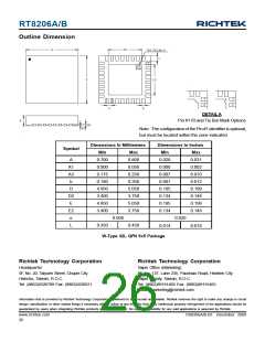
RT8206A/B
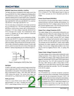
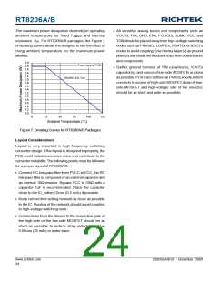
The maximum power dissipation depends on operating
ambient temperature for fixed TJ(MAX) and thermal
resistance θJA. For RT8206A/B packages, the Figure 7
of derating curves allows the designer to see the effect of
rising ambient temperature on the maximum power
allowed.
` All sensitive analog traces and components such as
VOUTx, FBx, GND, ENx, PGOODx, ILIMx, VCC, and
TONshould be placed away from high-voltage switching
nodes such as PHASEx, LGATEx, UGATEx or BOOTx
nodes to avoid coupling. Use internal layer(s) as ground
plane(s) and shield the feedback trace from power traces
and components.
3.0
2.8
Four Layers PCB
` Gather ground terminal of VIN capacitor(s), VOUTx
capacitor(s), and source of low-side MOSFETs as close
as possible. PCB trace defined as PHASEx node, which
connects to source of high-side MOSFET, drain of low-
side MOSFET and high-voltage side of the inductor,
should be as short and wide as possible.
2.6
2.4
2.2
WQFN -32L 5x5
2.0
1.8
1.6
1.4
1.2
1.0
0.8
0.6
0.4
0.2
0.0
0
25
50
75
100
125
Ambient Temperature (°C)
Figure 7.Derating Curves for RT8206A/B Packages
Layout Considerations
Layout is very important in high frequency switching
converter design. If the layout is designed improperly, the
PCB could radiate excessive noise and contribute to the
converter instability. The following points must be followed
for a proper layout of RT8206A/B.
` Connect RC low-pass filter from PVCC to VCC, the RC
low-pass filter is composed of an external capacitor and
an internal 10Ω resistor. Bypass VCC to GND with a
capacitor 1uF is recommended. Place the capacitor
close to the IC, within 12mm (0.5 inch) if possible.
` Keep current limit setting network as close as possible
to the IC. Routing of the network should avoid coupling
to high-voltage switching node.
` Connections from the drivers to the respective gate of
the high-side or the low-side MOSFET should be as
short as possible to reduce stray inductance. Use
0.65mm (25 mils) or wider trace.
www.richtek.com
24
DS8206A/B-03 December 2009

 RICHTEK [ RICHTEK TECHNOLOGY CORPORATION ]