RT8206A/B
LDO causes large power dissipation on automatic
switches, which may result in thermal shutdown.
⎡
⎤
R1
R2
⎛
⎜
⎝
⎞
⎟
⎠
V
OUTx
= V
× 1+
FBx
⎢
⎣
⎥
⎦
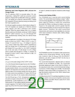
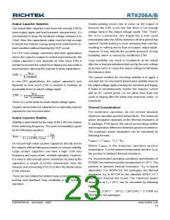
Where VFBx is 2V (typ.).
Discharge Mode
V
IN
When standby or shutdown mode occurs, or the output
under voltage fault latch is set, the outputs discharge mode
is triggered. During discharge mode, the output capacitor
will be discharged toGNDthrough an internal 20Ω switch.
V
OUTx
UGATEx
PHASEx
LGATEx
R1
R2
VOUTx
FBx
Shutdown Mode
GND
The RT8206A/B SMPS1, SMPS2 and LDO have
independent enabling control.Drive ENLDO, EN1 and EN2
below the precise input falling-edge trip level to place the
RT8206A/B in its low-power shutdown state. The
RT8206A/B consumes only 20uA of quiescent current while
in shutdown. When shutdown mode is activated, the
reference turns off. The accurate 1V falling-edge threshold
on the ENLDO can be used to detect a specific analog
voltage level and shutdown the device. Once in shutdown,
the 1.6V rising-edge threshold activates, providing sufficient
hysteresis for most application.
Figure 6. Setting VOUTx with a Resistor-Divider
Output Inductor Selection
The switching frequency (on-time) and operating point (%
ripple or LIR) determine the inductor value as follows :
T
L
×(V - V
)
ON
IN
OUT
L =
×I
IR LOAD(MAX)
Where LIR is the ratio of the peak-to-peak ripple current
to the average inductor current.
Find a low-loss inductor having the lowest possible DC
resistance that fits in the allotted dimensions. Ferrite cores
are often the best choice, although the powdered iron is
inexpensive and can work well at 200kHz. The core must
be large enough to prevent it from saturating at the peak
inductor current (IPEAK) :
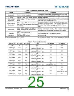
Power-Up Sequencing and On/Off Controls (ENx)
EN1 and EN2 control SMPS power-up sequencing. When
the RT8206A/B applies in the single channel mode, EN1
or EN2 enables the respective outputs when ENx voltage
rising above 2.5V, and disables the respective outputs
when ENx voltage falling below 1.8V.
IPEAK = ILOAD(MAX) + [(LIR / 2) x ILOAD(MAX)
]
Connecting one of ENx to VCC and the other one to REF
can force the latter one output starts after the former one
regulates.
This inductor ripple current also impacts transient-response
performance, especially at low VIN − VOUTx differences.
Low inductor values allow the inductor current to slew
faster, replenishing charge removed from the output filter
capacitors by a sudden load step. The peak amplitude of
the output transient. The VSAG also features a function of
the output transient (VSAG) is also a function of the
maximum duty factor, which can be calculated from the
on-time and minimum off-time :
If both of ENx forced to connect to REF, both outputs will
always wait for the regulation of the other one. However,
in this situation, neither of the two ENx will be in regulation.
Output Voltage Setting (FBx)
Connect FB1 directly toGNDor VCC for a fixed 5V output
(VOUT1). Connect FB2 directly toGNDor VCC for a fixed
3.3V output (VOUT2).
V
⎛
⎝
⎞
⎟
⎠
)2 ×L× K
+ T
OFF(MIN)
OUTx
V
IN
(ΔI
LOAD
⎜
V
SAG
=
⎡
⎛
⎤
V
IN
− V
OUTx
V
IN
⎞
⎟
⎠
The output voltage can also be adjusted from 2V to 5.5V
with a resistor-divider network (Figure 6). The following
equation is for adjusting the output voltage. Choose R2 to
be approximately 10kΩ, and solve for R1 using the following
equation :
2× C
× V
× K
− T
OFF(MIN)
OUT
OUTx
⎜
⎢
⎥
⎝
⎣
⎦
Where minimun off-time (TOFF(MIN)) = 300ns (typ.) and K
is from Table 1.
www.richtek.com
22
DS8206A/B-03 December 2009

 RICHTEK [ RICHTEK TECHNOLOGY CORPORATION ]