RT8206A/B
Output Capacitor Selection
Double-pulsing occurs due to noise on the output or
because the ESR is too low that there is not enough
voltage ramp in the output voltage signal. This “fools”
the error comparator into triggering a new cycle
immediately after the 300ns minimum off-time period has
expired. Double-pulsing is more annoying than harmful,
resulting in nothing worse than increased output ripple.
However, it may indicate the possible presence of loop
instability, which is caused by insufficient ESR.
The output filter capacitor must have low enough ESR to
meet output ripple and load-transient requirements, it’s
commanded to keep the feedback voltage between 6 to
12mV. Also, the capacitance value must be high enough
to absorb the inductor energy going from a full-load to no-
load condition without tripping the OVP circuit.
For CPU core voltage converters and other applications
where the output is subject to violent load transients, the
output capacitor’s size depends on how much ESR is
needed to prevent the output from dipping too low under a
load transient. Ignoring the sag due to finite capacitance :
Loop instability can result in oscillations at the output
after line or load perturbations that can trip the over-voltage
protection latch or cause the output voltage to fall below
the tolerance limit.
V
P-P
ESR ≤
I
LOAD(MAX)
The easiest method for checking stability is to apply a
very fast zero-to-max load transient and carefully observe
the output-voltage-ripple envelope for overshoot and ringing.
It helps to simultaneously monitor the inductor current
with an AC current probe. Do not allow more than one
cycle of ringing after the initial step-response under- or
overshoot.
In non-CPU applications, the output capacitor's size
depends on how much ESR is needed to maintain an
acceptable level of output voltage ripple :
V
P-P
ESR ≤
L
×I
IR LOAD(MAX)
There VP-P is the peak-to-peak output voltage ripple.
Organic semiconductor capacitor(s) or specialty polymer
capacitor(s) are recommended.
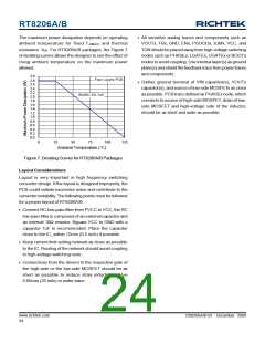
Thermal Considerations
For continuous operation, do not exceed absolute
maximum operation junction temperature. The maximum
power dissipation depends on the thermal resistance of
IC package, PCB layout, the rate of surroundings airflow
and temperature difference between junction to ambient.
The maximum power dissipation can be calculated by
following formula :
Output Capacitor Stability
Stability is determined by the value of the ESR zero relative
to the switching frequency. The point of instability is given
by the following equation :
fSW
4
1
fESR
=
≤
2×π ×ESR×COUT
PD(MAX) = ( TJ(MAX) - TA ) / θJA
Do not put high-value ceramic capacitors directly across
the outputs without taking precautions to ensure stability.
Large ceramic capacitors can have a high- ESR zero
frequency and cause erratic, unstable operation. However,
it is easy to add enough series resistance by placing the
capacitors a couple of inches downstream from the
inductor and connecting VOUTx or the FBx divider close
to the inductor.
Where TJ(MAX) is the maximum operation junction
temperature, TAis the ambient temperature and the θJA is
the junction to ambient thermal resistance.
For recommended operating conditions specification of
RT8206, the maximum junction temperature is 125°C. The
junction to ambient thermal resistance θJA is layout
dependent. For WQFN-32L 5x5 packages, the thermal
resistance θJA is 36°C/W on the standard JEDEC 51-7
four layers thermal test board. The maximum power
dissipation at TA = 25°C can be calculated by following
formula :
There are two related but distinct ways including double-
pulsing and feedback loop instability in the unstable
operation.
PD(MAX) = (125°C − 25°C) / (36°C/W) = 2.778W for
WQFN-32L 5x5 packages
DS8206A/B-03 December 2009
www.richtek.com
23

 RICHTEK [ RICHTEK TECHNOLOGY CORPORATION ]