RX62N Group, RX621 Group
3. Address Space
3.
Address Space
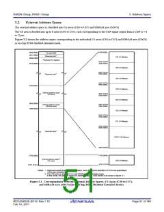
3.1
Address Space
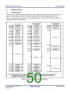
This LSI has a 4-Gbyte address space, consisting of the range of addresses from 0000 0000h to FFFF FFFFh. That is,
linear access to an address space of up to 4 Gbytes is possible, and this contains both program and data areas.
Figure 3.1 shows the memory maps in the respective operating modes. Accessible areas will differ according to the
operating mode and states of control bits.
On-chip ROM enabled
extended mode
On-chip ROM disabled
extended mode
2
Single-chip mode*
0000 0000h
0001 8000h
0008 0000h
0000 0000h
0001 8000h
0000 0000h
0001 8000h
0008 0000h
On-chip RAM
On-chip RAM
On-chip RAM
1
1
Reserved area*
Reserved area*
Reserved area*1
0008 0000h
Peripheral I/O registers
Peripheral I/O registers
Peripheral I/O registers
0010 0000h
0010 8000h
0010 0000h
0010 0000h
0010 8000h
On-chip ROM
(data flash)
On-chip ROM
(data flash)
Reserved area*1
FCU-RAM*3
Reserved area*1
3
FCU-RAM*
007F 8000h
007F A000h
007F 8000h
007F A000h
1
Reserved area*
Reserved area*1
007F C000h
007F C500h
007F C000h
007F C500h
Peripheral I/O registers
Peripheral I/O registers
Reserved area*1
1
1
Reserved area*
Reserved area*
007F FC00h
0080 0000h
007F FC00h
0080 0000h
Peripheral I/O registers
Reserved area*1
Peripheral I/O registers
Reserved area*1
00F8 0000h
0100 0000h
00F8 0000h
0100 0000h
On-chip ROM (program ROM)
(write only)
On-chip ROM (program ROM)
(write only)
0100 0000h
External address space
(CS area)
External address space
(CS area)
0800 0000h
1000 0000h
0800 0000h
1000 0000h
External address space
(SDRAM area)
External address space
(SDRAM area)
Reserved area*1
1
Reserved area*
1
Reserved area*
FEFF E000h
3
FEFF E000h
3
On-chip ROM (FCU firmware)*
(read only)
On-chip ROM (FCU firmware)*
(read only)
FF00 0000h
FFFF FFFFh
FF00 0000h
FF7F C000h
FF80 C000h
FF00 0000h
FF7F C000h
FF80 C000h
1
1
Reserved area*
Reserved area*
On-chip ROM (user boot)
(read only)
On-chip ROM (user boot)
(read only)
External address space
Reserved area*1
Reserved area*1
FFF8 0000h
FFFF FFFFh
FFF8 0000h
FFFF FFFFh
On-chip ROM (program ROM)
(read only)
On-chip ROM (program ROM)
(read only)
Notes: 1. Reserved areas should not be accessed, since the correct operation of LSI is not guaranteed if they are accessed.
2. The address space in boot mode and user boot mode is the same as the address space in single-chip mode.
3. For details on the FCU, see section 37, ROM (Flash Memory for Code Storage) and section 38, Data Flash
(Flash Memory for Data Storage) in the User’s manual: Hardware.
Figure 3.1 Memory Map in Each Operating Mode
R01DS0052EJ0110 Rev.1.10
Feb 10, 2011
Page 50 of 146

 RENESAS [ RENESAS TECHNOLOGY CORP ]