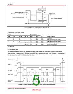
M61880FP
Charging constant-
current source
Comparator
Reference voltage input
SW1
Output (CH pin)
RM resistance generation voltage
Control circuit
S/H
SW2
Sample-and-hold control input
External capacitance
CH
Discharging constant-
current source
ENB
Tr1
Conceptual Diagram of Sample-and-Hold Circuit
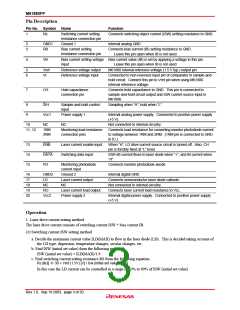
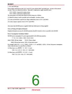
Operation Function Table
Input
Switch State
ENB
H
S/H
X
DATA
VM, Vr
SW1
OFF
OFF
OFF
ON
SW2
OFF
OFF
OFF
OFF
ON
Tr1
Output (CH Pin)
X
X
H
L
X
ON
Fixed at “L”
L
H
X
OFF
OFF
OFF
OFF
High-impedance state (hold)
High-impedance state (hold)
Current source (sample)
Current sink (sample)
L
L
X
VM < Vr
VM > Vr
OFF
X: Don’t Care
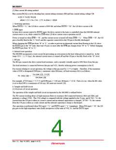
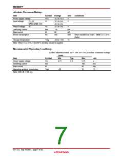
(2) APC timing chart
An example of a timing chart of APC operation by means of the sample-and-hold control signals is shown below.
In this example, a case is shown in which the direction of the CH pin leakage current in the hold state is assumed to be
the direction of flow to the M61880 (forward direction).
Power supply
ENB input
Sample
Sample
Sample
Hold
Hold
Hold
S/H input
DATA input
∆ILD
Laser drive
current
Example of Sample-and-Hold Type APC Circuit Operation Timing Chart
Rev.1.0, Sep.19.2003, page 5 of 20

 RENESAS [ RENESAS TECHNOLOGY CORP ]