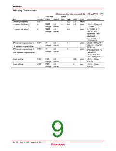
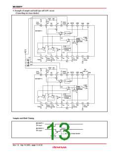
M61880FP
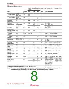
Switching Characteristics
(Unless specified otherwise noted, Ta = 25ºC and VCC = 5 V)
Test Pins
Symbol Input
Limits
Item
Output Min. Typ.
Max.
2.0
Unit
Test Conditions
Operating frequency
LD current rise time (*)
fop
tr
100
Mbps
nsec
DATA
voltage current
DATA LD
voltage current
LD
1.0
2.0
ILD (H) = 50mA, ILD
(L) = 0mA
Rs = 840Ω, CH =
0.047µF, APC
adjustment; RM =
adjustment
LD current fall time (*)
tf
1.0
nsec
(CH = 2.5V), Vr =
1.5V (Note 1)
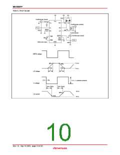
APC circuit response time 1
tRP1
tRP2
Vr
LD
1
3
µsec
µsec
ILD (H) = 50mA, Rs =
840Ω, CH = 0.047µF,
DATA = 0V
APC adjustment; RM
= adjustment
voltage current
(1% variance response time)
APC circuit response time 2
Vr
LD
voltage current
(50% variance response time)
(CH = 2.5V), Vr =
1.5V ± 0.5% (Note 1)
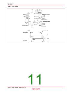
Circuit on time
Circuit off time
tON
ENB
voltage current
ENB LD
voltage current
LD
350
5
µsec
µec
ILD (H) = 50mA
(Note 2)
tOFF
ILD (H) = 50mA
(Note 2)
Rev.1.0, Sep.19.2003, page 9 of 20

 RENESAS [ RENESAS TECHNOLOGY CORP ]