M61880FP
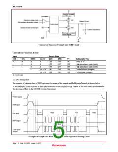
Block Diagram
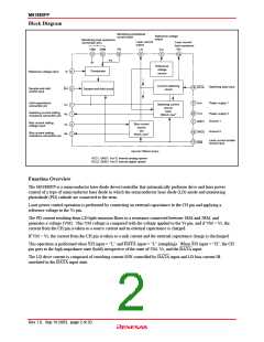
Monitoring photodiode
current input
Reference voltage
output
Monitoring load resistance
connection pins
Laser current
output
Laser current
load resistance
RO
1RM
11
2RM
12
PD
15
LD
Vref
17
5
19
I
PD
Reference
voltage
source
Comparator
6
8
Reference voltage input
Vr
Current switching
circuit
Switching data input
Power supply 1
14 DATA
Sample-and-hold
control input
S/H
Sample-and-hold circuit
Hold capacitance
connection pin
9 VCC1
Switching current
source
(Isw)
100mA max
C
H
S
7
1
Switching current setting
resistance connection pin
20 VCC2
Power supply 2
Ground 1
R
GND1
GND2
ENB
2
Bias current setting
voltage input
Bias current
source
V
B
4
3
(I
B)
Ground 2
16
13
Bias current setting
resistance connection pin
RB
40mA max
Laser current enable
control input
I
SW+IB=100mA (max)
VCC1, GND1: For IC internal analog system
VCC2, GND2: For IC internal digital system
Function Overview
The M61880FP is a semiconductor laser diode driver/controller that automatically performs drive and laser power
control of a type of semiconductor laser diode in which the semiconductor laser diode (LD) anode and monitoring
photodiode (PD) cathode are connected to the stem.
Laser power control operation is performed by connecting an external capacitance to the CH pin and applying a
reference voltage to the Vr pin.
The PD current resulting from LD light emission flows to a resistance connected between 1RM and 2RM, and
generates a voltage (VM). This VM voltage is compared with the voltage applied to the Vr pin, and if VM < Vr, the
current from the CH pin is taken as a source current and an external capacitance is charged.
If VM > Vr, the current from the CH pin is taken as a sink current and the external capacitance charge is discharged.
This operation is performed when S/H input = “L” and DATA input = “L” (sampling). When S/H input = “H”, the CH
pin goes to the high-impedance state (hold) irrespective of the state of VM, Vr, and the DATA input.
The LD drive current is composed of switching current ISW controlled by DATA input and LD bias current IB
unrelated to the DATA input state.
Rev.1.0, Sep.19.2003, page 2 of 20

 RENESAS [ RENESAS TECHNOLOGY CORP ]