M61880FP
(2) Bias current IB setting method
Bias current IB [A] is set by deciding bias current setting resistance RB and bias current setting voltage VB.
I
B
[A]
V
B
[A] / R
B
[Ω]
where 1.2 V ≤ V
B
≤ Vcc - 2.7V, IB (max.) = 40mA
2. Switching operation
When DATA = “L”, the LD drive current is ISW+IB, and when DATA = “H”, the LD drive current is IB.
3. ENB input
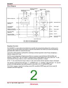
In laser drive current control by DATA input, the drive current to the laser is controlled when the M61880 internal
current source is on, while control by ENB turns LD drive current source operation on/off.
Power is turned on when ENB = “H”, and the current secure is turned off when ENB = “L”. When ENB = “H”, the CH
pin is forcibly fixed at the “L” level, and the capacitor connected to the CH pin is forcibly discharged.
When changing the ENB pin from “H” to “L”, in order to prevent an abnormal current from flowing in the LD, drive
the DATA pin to the “H” state, then wait 10 µsec or more after the ENB pin changes from “H” to “L” before changing
the DATA pin from “H” to “L”.
4. Internal reset operation
The M61880 incorporates a reset circuit for preventing an overcurrent in the laser when power is turned on. In the
range VCC < 3.5 V (typ.), the internal current source is turned off and the CH pin is forcibly fixed at the “H” level.
5. RO pin
The RO pin connects the drive current load resistance, and a currently virtually equal to ISW flows from this pin.
The load resistance is connected between this pin and VCC, thereby reducing power consumption in the IC.
For reasons relating to circuit operation, the voltage at this pin must be 2.5 V or higher. Therefore, if the maximum
value of ISW is designated ISW(max.), maximum value RO(max.) of load resistance RO is as follows:
Vcc (min.) [V] - 2.5 [V]
RS (max.) [Ω] =
I
SW (max.) [A]
For example, if VCC(min.) = 4.75 V and ISW(max.) = 100 mA, RO(max.) = 22 Ω. That is to say, when the RS value
is set so that ISW is a maximum of 100 mA, RO must not exceed 22Ω.
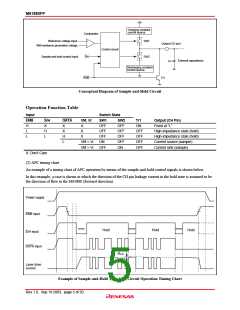
6. Sample-and-hold circuit
(1) Overview of circuit operation
The operation of the sample-and-hold circuit incorporated in the M61880 is outlined below.
The PD current resulting from LD light emission flows to resistance RM connected between 1RM and 2RM, and
generates a voltage (VM). This VM voltage is compared with the voltage applied to the Vr pin, and if VM < Vr, the
current from the CH pin is taken as a source current and an external capacitance is charged. If VM > Vr, the current
from the CH pin is taken as a sink current and the external capacitance charge is discharged.
This operation is performed when S/H input = “L” and DATA input = “L” (sampling). When S/H input = “H”, the CH
pin goes to the high-impedance state (hold) irrespective of the state of VM, Vr, and the DATA input.
Rev.1.0, Sep.19.2003, page 4 of 20

 RENESAS [ RENESAS TECHNOLOGY CORP ]