M37161M8/MA/MF-XXXSP/FP,M37161EFSP/FP
Table 7.2 PIN DESCRIPTION (continued)
Input/
Pin
Name
Functions
Output
Input
Input
Input
P50/HSYNC Input P5
Port P5 is a 2-bit input port.
P51/VSYNC Horizonta synchronous signal
Vertical synchronous signal
P50 pin is also used as a horizontal synchronous signal input HSYNC for OSD.
P51 pin is a vertical synchronous signal input VSYNC for OSD.
P52/B,
Output P5
output
output
Pins P52–P55 are 4-bit output port. The output structure is CMOS output.
Pins P52–P55 are also used as OSD output pins R, G, B and OUT respectively. The output
structure is CMOS output.
P53/G,
P54/R,
OSD output
P55/OUT
FILT
Clock oscillation
filter
Input
Connect a capacitor between FILT and Vss.
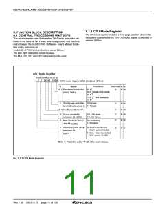
Notes : Port Pi (i = 0 to 3) has a port Pi direction register that can be used to program each bit for input (“0”) or an output (“1”). The pins programmed as “1” in the
direction register are output pins. When pins are programmed as “0,” they are input pins. When pins are programmed as output pins, the output data is
written into the port latch and then output. When data is read from the output pins, the data of the port latch, not the output pin level, is read. This allows a
previously output value to be read correctly even if the output LOW voltage has risen due to, for example, a directly-driven light emitting diode. The input pins
are in the floating state, so the values of the pins can be read. When data is written to the input pin, it is written only into the port latch, while the pin remains
in the floating state.
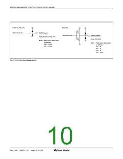
ꢀꢀꢀꢀLED drive ports 4 (P24–P27)
Rev.1.00 2003.11.25 page 8 of 128

 RENESAS [ RENESAS TECHNOLOGY CORP ]