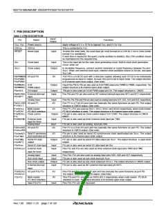
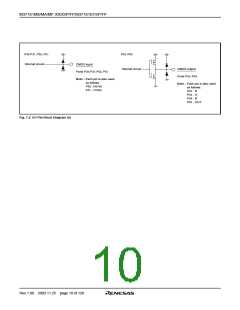
M37161M8/MA/MF-XXXSP/FP,M37161EFSP/FP
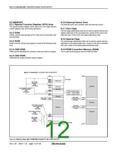
8.1.1 CPU Mode Register
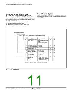
8. FUNCTION BLOCK DESCRIPTION
8.1 CENTRAL PROCESSING UNIT (CPU)
This microcomputer uses the standard 740 Family instruction set.
Refer to the table of 740 Family addressing modes and machine
instructions or the SERIES 740 <Software> User’s Manual for de-
tails on the instruction set.
The CPU mode register includes a stack page selection bit and inter-
nal system clock selection bit. The CPU mode register is allocated at
address 00FB16.
Availability of 740 Family instructions are as follows:
The FST, SLW instruction cannot be used.
The MUL, DIV, WIT and STP instructions can be used.
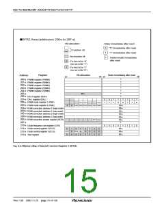
CPU Mode Register
b7b6 b5b4b3 b2b1b0
1 1
0 0
CPU mode register (CM) [Address 00FB16
]
Functions
After reset
0
B
Name
R W
R W
b1 b0
Processor mode bits
(CM0, CM1)
0, 1
0 0: Single-chip mode
0 1:
1 0:
1 1:
Not available
0: 0 page
1: 1 page
Stack page selection
bit (CM2) (See note1)
2
1
R W
Fix these bits to “1.”
1
1
R W
R W
3, 4
5
0: LOW drive
1: HIGH drive
X
COUT drivability
selection bit (CM5)
6
7
0
0
R W
R W
0: Oscillating
1: Stopped
Main Clock (XIN-XOUT
)
stop bit
(CM6)
Internal system clock 0:
selection bit
X
IN-XOUT selected
(high-speed mode)
1: XCIN–XCOUT selected
(low-speed mode)
(CM7)
Note 1: This bit is set to “1” after the reset release.
Fig. 8.1.1 CPU Mode Register
Rev.1.00 2003.11.25 page 11 of 128

 RENESAS [ RENESAS TECHNOLOGY CORP ]