M37161M8/MA/MF-XXXSP/FP,M37161EFSP/FP
7. PIN DESCRIPTION
Table 7.1 PIN DESCRIPTION
Input/
Output
Pin
Name
Functions
VCC, VSS
Power source
CNVSS
Apply voltage of 5 V ± 10 % to (typical) VCC, and 0 V to VSS.
This is connected to VSS.
CNVSS
______
RESET
Reset input
Input
To enter the reset state, the reset input pin must be kept at a LOW for 2 ms or more (under
normal VCC conditions).
If more time is needed for the quartz-crystal oscillator to stabilize, this LOW condition should
be maintained for the required time.
XIN
Clock input
Input
This is the input pin for the main clock generating circuit. Built-in clock clock generation
circuit, when set
XOUT
Clock output
Output
to oscillation frequency, connect ceramic resonator or crystal frequency between XIN and
XOUT. When use external clock input, connect clock oscillation source to XIN pin, and open
XOUT pin.
P0
P0
P0
0
/PWM0/DA I/O port P0
/PWM1,
/PWM2,
I/O
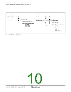
Port P0 is a 8-bit I/O port with a direction register allowing each I/O bit to be individually
programmed as input or output. At reset, this port is set to input mode. The output structure
is N-channel open-drain output. (See note)
1
2
P03/PWM3/AD1, 8-bit
P0 /PWM4/AD2, PWM output
Output
Ouput Pins P00 to P04 are also used as 8-bit PWM output pins PWM0 to PWM4, respectively. The
output structure is N-channel open-drain output.
4
P05/AD3,
DA output
Output
Input
P00 pin is also used as 14-bit PWM output pin DA. The output structure is CMOS.
P06/INT2/AD4, External interrupt
Pins P0
6
and P0
7
are also used as INT external interrupt input pins INT2 and INT1 respectively.
P07/INT1
input
Analog input
Input
I/O
Pins P03, P04, P0
5
and P0 are also used as analog input pins AD1, AD2, AD3 and AD4, respectively.
6
P1
0
/CLK CONT, I/O port P1
Port P1 is a 7-bit I/O port and has basically the same functions as port P0. The output
structure is CMOS output. (See note)
P11/SCL1,
P12/SCL2, Multi-master
I/O
Pins P11–P14 are used as SCL1, SCL2, SDA1 and SDA2 respectively, when multi-master
I C-BUS interface is used. The output structure is N-channel open-drain output.
2
2
P13/SDA1
I C-BUS interface
,
P14/SDA2, Clock control
P15
Output
Input
P10 pin is also used as Clock control output CLK CONT. The output structure is CMOS
output.
,
P16
/
AD8/TIM2 External clock
P16 pin is also used as timer external clock input pin TIM2.
input for timer
Analog input
Input
I/O
P16 pin is also used as analog input pin AD8.
P20
/SCLK/AD5, I/O port P2
/AD6
Port P2 is a 8-bit I/O port and has basically the same functions as port P0. The output
structure is CMOS output. (See note)
P21
/SOUT
,
P2
2
/SIN/AD7, Serial I/O synchronous
I/O
P20 pin is also used as serial I/O synchronous clock input/output pin SCLK. The output
structure is N-channel open-drain output.
clock input/output port
P23/TIM3,
P24/TIM2,
/INT3
P25
Serial I/O data
output
Output
P21 pin is also used as serial I/O data output pin SOUT. The output structure is open-drain
output.
,
P2
6
/
XCIN,
Serial I/O data input
Input
Input
P22 pin is also used as serial I/O data input pin SIN.
P27/XCOUT External clock
input for timer
Pins P23 and P24 are also used as timer external clock input pins TIM3 and TIM2
respectively.
Analog input
Input
Input
Pins P20–P22 are also used as analog input pins AD5, AD6 and AD7 respectively.
P26 pin is also used as sub-clock input pin XCIN.
Sub-clock input
Sub-clock output
External interrupt
input
Output
Input
P27 pin is also used as sub-clock output pin XCOUT. The output structure is CMOS output.
P25 pin is also used as INT external interrupt input pin INT3.
P30/SDA3 I/O port P30, P31
P31/SCL3
I/O
I/O
Pins P30 and P31 are 2-bit I/O port and has basically the same functions as port P0.
The output structure is CMOS output. (See note)
2
P35-P37
Multi-master
2
Pins P30 and P31 are used as SDA3,SCL3 respectively, when multi-master I C-BUS
I C-BUS Interface
interface is used. The output structure is N-channel open-drain output.
Input P35-P37
Input
Pins P35–P37 are 3-bit input port.
Rev.1.00 2003.11.25 page 7 of 128

 RENESAS [ RENESAS TECHNOLOGY CORP ]