M37161M8/MA/MF-XXXSP/FP,M37161EFSP/FP
6. PERFORMANCE OVERVIEW
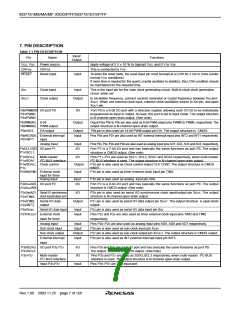
Table 6.1 Performance Overview
Parameter
Functions
71
Number of basic instructions
Instruction execution time
0.5 ms (the minimum instruction execution time, at 8 MHz oscillation fre-
quency)
Clock frequency
8 MHz (maximum)
ROM M37161M8-XXXSP/FP
Memory size
32K bytes
M37161MA-XXXSP/FP
M37161MF-XXXSP/FP,M37161EFSP/FP
RAM M37161M8-XXXSP/FP
M37161MA/MF-XXXSP/FP,M37161EFSP/FP
OSD ROM
40K bytes
60K bytes
1152 bytes (ROM correction memory included)
1472 bytes (ROM correction memory included)
20K bytes
OSD RAM
128 bytes
P0
8-bit ꢀ 1 (N-channel open-drain output structure, can be used as 8-bit PWM
output pins, INT input pins, A-D input pin, 14-bit PWM output pins. How-
ever, CMOS output structure, when P00 is used as serial output.)
Input/Output
ports
I/O
I/O
7-bit ꢀ 1 (CMOS input/output structure, however, N-channel open-drain
P10–P16
P20–P27
P30, P31
2
output structure, when P11–P14 are used as multi-master I C-BUS inter-
face, can be used as A-D input pins, timer external clock input pins, multi-
2
master I C-BUS interface)
8-bit ꢀ 1 (P2 is CMOS input/output structure, however, N-channel open-
drain output structure when P20 and 21 are used as serial output, can be
used as serial input/output pins, timer external clock input pins, A-D input
pins, INT input pin, sub-clock input/output pins)
I/O
2-bit ꢀ 1 (CMOS input/output structure, however, N-channel open-drain out-
I/O
2
put structure, when used as multi-master I C-BUS interface, can be used as
2
multi-master I C-BUS interface.)
P35-P37
P50, P51
P52–P55
3-bit ꢀ 1
Input
2-bit ꢀ 1 (can be used as OSD input pins)
4-bit ꢀ 1 (CMOS output structures, can be used as OSD output pins)
Input
Output
Serial I/O
8-bit ꢀ 1
2
Multi-master I C-BUS interface
A-D comparator
One (Three lines)
8 channels (7-bit resolution)
14-bit ꢀ 1, 8-bit ꢀ 5
PWM output circuit
Timers
8-bit ꢀ 6
2 vectors
ROM correction function
Subroutine nesting
Interrupt
128 levels (maximum)
<16 types>
INT external interrupt ꢀ 3, Internal timer interrupt ꢀ 6, Serial I/O interrupt ꢀ
2
1, OSD interrupt ꢀ 1, Multi-master I C-BUS interface interrupt ꢀ 1, f(XIN)/
4096 interrupt ꢀ 1, VSYNC interrupt ꢀ 1, BRK instruction interrupt ꢀ 1, reset
ꢀ 1
Clock generating circuit
2 built-in circuits (externally connected to XCIN/OUT is a ceramic resonator
or a quartz-crystal oscillator)
Rev.1.00 2003.11.25 page 5 of 128

 RENESAS [ RENESAS TECHNOLOGY CORP ]