M37161M8/MA/MF-XXXSP/FP,M37161EFSP/FP
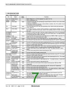
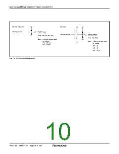
Ports P00–P07
Direction register
Port latch
N-channel open-drain output
Ports P00–P07
Data bus
Note : Each port is also used as follows :
P00 : DA/PWM0
P01–P04 : PWM1–PWM4
P05: AD3
P06: INT2/AD4
P07: INT1
Ports P1, P2, P30, P31
Direction register
Port latch
CMOS output
Data bus
Ports P1, P2, P30, P31
Notes 1: Each port is also used as follows :
P10 : CLKCONT
P11 : SCL1
P12 : SCL2
P20 : SCLK/AD5
P21 : SOUT/AD6
P22 : SIN/AD7
P23 : TIM3
P27 : XCOUT
P30 : SDA3
P31 : SCL3
P13 : SDA1
P14 : SDA2
P24 : TIM2
P16 : AD8/TIM2
P25 : INT3
P26 : XCIN
2: The output structure of ports P11–P14, P30–P31 is N-channel open-drain output when using as multi-master
2
I C-BUS interface (it is the same with P00–P07).
3: The output structure of ports P20 and P21 is N-channel open-drain output when using as serial output (it is the
same as P00–P07).
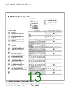
Fig. 7.1 I/O Pin Block Diagram (1)
Rev.1.00 2003.11.25 page 9 of 128

 RENESAS [ RENESAS TECHNOLOGY CORP ]