M37161M8/MA/MF-XXXSP/FP,M37161EFSP/FP
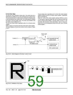
8.10.2 Dot Size
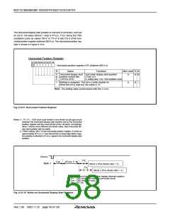
The pre-divide ratio is specified by bit 7 of the OSD control register
(address 00D016) and bit 4 of block control register i (addresses
00D216 and 00D316) .
The dot size can be selected in block units. The vertical dot size is
determined by dividing HSYNC in the vertical dot size control circuit.
The horizontal dot size in is determined by dividing the following clock
in the horizontal dot size control circuit : the clock gained by dividing
the f(OSC) in the pre-divide circuit. The clock cycle divided in the
pre-divide circuit is defined as 1TC.
When bit 7 of the OSD control register (address 00D016) is set to
"0," the double or triple pre-divide ratio can be chosen per block unit
by bit 4 of block control register i. And then, when it is set to "1", the
pre-divide ratio increases 1 time (both blocks 1 and 2). The pre-di-
vided dot size can be specified per block unit by bits 2 and 3 of block
control register i.
The dot size of each block is specified by bits 2 to 4 of block control
register i.
Refer to Figure 8.10.4 for the structure of the block control register.
The block diagram of the dot size control circuit is shown in Figure
8.10.11.
Clock cycle
= 1TC
“0”
“1”
Synchronous
circuit
f (OSC)
Horizontal dot size
control circuit
Cycle ✕ 2
Cycle ✕ 3
OC7
“1”
“0”
BCi4
Pre-divide circuit
Vertical dot size
control circuit
HSYNC
OSD control circuit
Fig. 8.10.11. Block Diagram of Dot Size Control Circuit
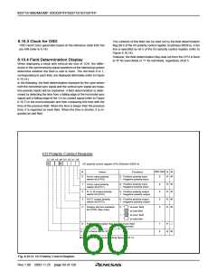
1 dot
1T
C
1T
C
2T
C
3TC
Scanning line of F1(F2 )
Scanning line of F2(F1 )
1/2 H
1H
2H
3H
Fig. 8.10.12 Definition of Dot Sizes
Rev.1.00 2003.11.25 page 59 of 128

 RENESAS [ RENESAS TECHNOLOGY CORP ]