M37161M8/MA/MF-XXXSP/FP,M37161EFSP/FP
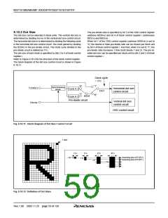
8.10.3 Clock for OSD
The contents of this field can be read out by the field determination
flag (bit 6 of the I/O polarity control register at address 00D816). A dot
line is specified by bit 5 of the I/O polarity control register (refer to
Figure 8.10.14).
OSD clock f (osc) generated based on the reference clock from the
pin XIN.(refer to 8.14)
However, the field determination flag read out from the CPU is fixed
to “0” for even fields or “1” for odd fields, regardless of bit 5.
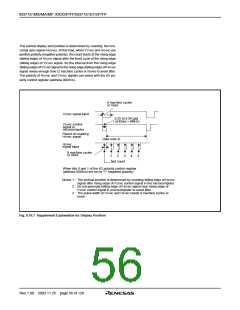
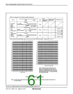
8.10.4 Field Determination Display
When displaying a block with vertical dot size of 1/2H, the differ-
ences in the synchronizing signal waveform of the interlacing system
determine whether the field is odd or even. The dot lines 0 or 1,
vorresponding to each field, are displayed alternately (refer to Figure
8.10.14.)
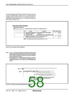
In the following, the field determination standard for the case where
both the horizontal sync signal and the vertical sync signal are nega-
tive-polarity inputs will be explained. A field determination is deter-
mined by detecting the time from a falling edge of the horizontal sync
signal until a falling edge of the VSYNC control signal (refer to Figure
8.10.7) in the microcomputer and then comparing this time with the
time of the previous field. When the time is longer than the previous
time, it is regarded as even field. When the time is shorter, it is re-
garded as odd field
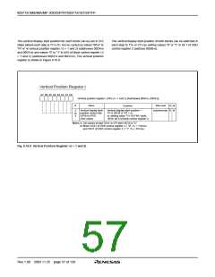
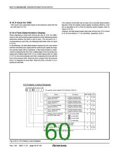
I/O Polarity Control Register
b7 b6 b5 b4 b3 b2 b1 b0
0
0
I/O polarity control register (PC) [Address 00D816
]
After reset
0
B
0
Name
Functions
R
R
W
W
H
SYNC input polarity
switch bit (PC0)
0 : Positive polarity input
1 : Negative polarity input
1
2
3
5
0 : Positive polarity input
1 : Negative polarity input
0
0
0
0
R
R
R
R
W
W
W
W
V
SYNC input polarity
switch bit (PC1)
0 : Positive polarity output
1 : Negative polarity output
R, G, B output polarity
switch bit (PC2)
OUT1 output polarity
switch bit (PC3)
0 : Positive polarity output
1 : Negative polarity output
Display dot line selection
bit (PC5) (See note)
0 : “
” at even field
” at odd field
” at even field
” at odd field
“
1 : “
“
6
Field determination flag
(PC6)
0 : Even field
1 : Odd field
1
0
R
R
—
4, 7
Fix these bits to “0.”
W
Note: Refer to the corresponding figure. 8.10.14.
Fig. 8.10.13 I/O Polarity Control Register
Rev.1.00 2003.11.25 page 60 of 128

 RENESAS [ RENESAS TECHNOLOGY CORP ]