M37161M8/MA/MF-XXXSP/FP,M37161EFSP/FP
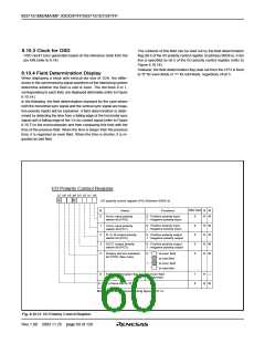
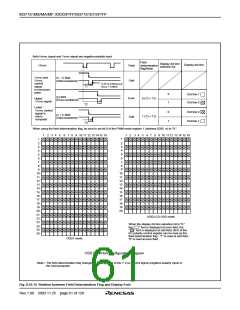
Both HSYNC cignal and VSYNC signal are negative-polarity input
Field
determination
flag(Note)
Display dot line
selection bit
Display dot line
H
SYNC
Field
Odd
V
V
SYNC and
SYNC
(n –1) field
(Odd-numbered)
control
0.25 to 0.50[ µs] at
T1
T2
T3
signal
in microcom-
puter
f(XIN) = 8 MHz
0
1
Dot line 1
Dot line 0
(n) field
(Even-numbered)
Even
Odd
0 (T2 > T1)
1 (T3 < T2)
Upper :
V
SYNC signal
Lower :
V
SYNC control
0
1
Dot line 0
Dot line 1
signal in
micro-
computer
(n +1) field
(Odd-numbered)
When using the field determination flag, be sure to set bit 0 of the PWM mode register 1 (address 0208 16) to “0.”
10 11 12 13 1415 16 9 10 1112 13 14 15 16
1
2
3
4
5
6
7
8
9
1
2
3
4
5
6 7 8
1
2
1
2
3
3
4
4
5
6
5
6
7
7
8
9
8
9
10
11
12
13
14
15
16
17
18
19
20
21
22
23
10
11
12
13
14
15
16
17
18
19
20
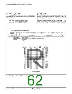
OSD2,CD OSD mode
When the display dot line selection bit is “0,”
24
25
the “
” font is displayed at even field, the
“
” font is displayed at odd field. Bit 6 of the
I/O polarity control register can be read as the
field determination flag : “1” is read at odd field,
“0” is read at even field.
26
OSD1 mode
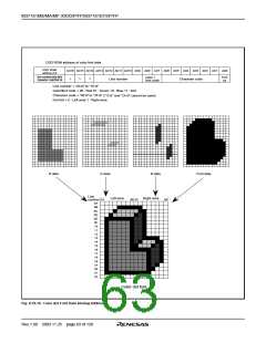
OSD ROM font configuration diagram
Note : The field determination flag changes at a rising edge of the V SYNC control signal (negative-polarity input) in
the microcomputer.
Fig. 8.10.14 Relation between Field Determination Flag and Display Font
Rev.1.00 2003.11.25 page 61 of 128

 RENESAS [ RENESAS TECHNOLOGY CORP ]