M37161M8/MA/MF-XXXSP/FP,M37161EFSP/FP
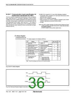
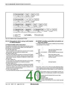
S
Slave address R/W
7 bits “0”
A
Data
A
Data
A/A
P
P
A
1 to 8 bits
1 to 8 bits
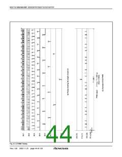
(1) A master-transmitter transmits data to a slave-receiver
R/W
“1”
S
Slave address
7 bits
A
Data
A
Data
A
1 to 8 bits
1 to 8 bits
(2) A master-receiver receives data from a slave-transmitter
Slave address
1st 7 bits
Slave address
2nd byte
S
R/W
“0”
A
A
Data
1 to 8 bits
Data
A/A
P
7 bits
8 bits
1 to 8 bits
(3) A master-transmitter transmits data to a slave-receiver with a 10-bit address
Slave address
1st 7 bits
Slave address
2nd byte
Slave address
1st 7 bits
S
R/W
“0”
A
A
Sr
R/W Data
A
Data
A
P
7 bits
8 bits
7 bits
“1” 1 to 8 bits
1 to 8 bits
(4) A master-receiver receives data from a slave-transmitter with a 10-bit address
S : START condition
A : ACK bit
Sr : Restart condition
P : STOP condition
R/W : Read/Write bit
From master to slave
From slave to master
Fig. 8.6.13 Address Data Communication Format
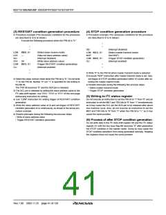
8.6.12 Precautions when using multi-master
(2) START condition generation procedure us-
ing multi-master
2
I C-BUS interface
✽ Procedure example (The necessary conditions for the procedure
(1) Read-modify-write instruction
Precautions for executing the read-modify-write instructions such as
are described in ✽ to ✽ below).
2
SEB and CLB, is executed for each register of the multi-master I C-
•
•
BUS interface are described below.
2
•I C data shift register (S0)
LDA
SEI
—
(Take out of slave address value)
(Interrupt disabled)
When executing the read-modify-write instruction for this register
during transfer, data may become an arbitrary value.
BBS 5,S1,BUSBUSY (BB flag confirmation and branch process)
BUSFREE:
STA S0
2
•I C address register (S0D)
When the read-modify-write instruction is executed for this register
(Write slave address value)
(Trigger START condition generation)
(Interrupt enabled)
at detection of the STOP condition, data may become an arbitrary
LDM #$F0, S1
______
value because hardware changes the read/write bit (RBW) at the
CLI
above timing.
•
•
2
•I C status register (S1)
Do not execute the read-modify-write instruction for this register
because all bits of this register are changed by hardware.
BUSBUSY:
CLI
(Interrupt enabled)
2
•I C control register (S1D)
•
•
When the read-modify-write instruction is executed for this register
at detection of the START condition of the byte transfer, data may
become an arbitrary value because hardware changes the bit
counter (BC0–BC2) at the above timing.
✽ Use “STA,” “STX” or “STY” of the zero page addressing instruc-
2
tion for writing the slave address value to the I C data shift register.
2
•I C clock control register (S2)
✽ Use “LDM” instruction for setting trigger of START condition gen-
eration.
The read-modify-write instruction can be executed for this register.
✽ Write the slave address value of ✽ and set trigger of START con-
dition generation as in ✽ continuously, as shown in the procedure
example.
✽ Disable interrupts during the following three process steps:
• BB flag confirmation
• Write slave address value
• Trigger of START condition generation
When the condition of the BB flag is bus busy, enable interrupts
immediately.
Rev.1.00 2003.11.25 page 40 of 128

 RENESAS [ RENESAS TECHNOLOGY CORP ]