M37161M8/MA/MF-XXXSP/FP,M37161EFSP/FP
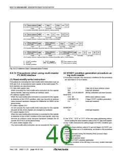
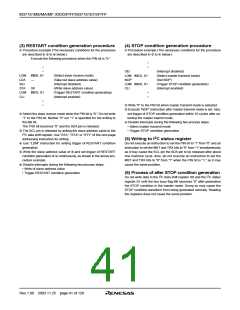
(3) RESTART condition generation procedure
✽ Procedure example (The necessary conditions for the procedure
are described in ✽ to ✽ below.)
(4) STOP condition generation procedure
✽ Procedure example (The necessary conditions for the procedure
are described in ✽ to ✽ below.)
Execute the following procedure when the PIN bit is “0.”
•
•
•
•
SEI
(Interrupt disabled)
LDM #$00, S1
(Select slave receive mode)
(Take out slave address value)
(Interrupt disabled)
LDM #$C0, S1
NOP
(Select master transmit mode)
(Set NOP)
LDA
SEI
—
LDM #$D0, S1
CLI
(Trigger STOP condition generation)
(Interrupt enabled)
STA
S0
(Write slave address value)
(Trigger RESTART condition generating)
(Interrupt enabled)
LDM #$F0, S1
•
CLI
•
•
•
✽ Write “0” to the PIN bit when master transmit mode is selected.
✽ Execute “NOP” instruction after master transmit mode is set. Also,
set trigger of STOP condition generation within 10 cycles after se-
lecting the master trasmit mode.
✽ Select the slave receive mode when the PIN bit is “0.” Do not write
“1” to the PIN bit. Neither “0” nor “1” is specified for the writing to
the BB bit.
✽ Disable interrupts during the following two process steps:
• Select master transmit mode
The TRX bit becomes “0” and the SDA pin is released.
✽ The SCL pin is released by writing the slave address value to the
• Trigger STOP condition generation
2
I C data shift register. Use “STA,” “STX” or “STY” of the zero page
2
addressing instruction for writing.
(5) Writing to I C status register
✽ Use “LDM” instruction for setting trigger of RESTART condition
generation.
Do not execute an instruction to set the PIN bit to “1” from “0” and an
instruction to set the MST and TRX bits to “0” from “1” simultaneously
as it may cause the SCL pin the SDA pin to be released after about
one machine cycle. Also, do not execute an instruction to set the
MST and TRX bits to “0” from “1” when the PIN bit is “1,” as it may
cause the same problem.
✽ Write the slave address value of ✽ and set trigger of RESTART
condition generation of ✽ continuously, as shown in the above pro-
cedure example.
✽ Disable interrupts during the following two process steps:
• Write of slave address value
• Trigger RESTART condition generation
(6) Process of after STOP condition generation
2
2
Do not write data in the I C data shift register S0 and the I C status
register S1 until the bus busy flag BB becomes “0” after generation
the STOP condition in the master mode. Doing so may cause the
STOP condition waveform from being generated normally. Reading
the registers does not cause the same problem.
Rev.1.00 2003.11.25 page 41 of 128

 RENESAS [ RENESAS TECHNOLOGY CORP ]