M37161M8/MA/MF-XXXSP/FP,M37161EFSP/FP
8.7 PWM OUTPUT FUNCTION
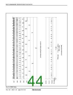
Figure 8.7.2 shows the 8-bit PWM timing. One cycle (T) is com
8
This microcomputer is equipped with five 8-bit PWMs (PWM0–
PWM4). PWM0–PWM4 have the same circuit structure, an 8-bit reso-
lution with minimum resolution bit width of 4 µs and repeat period of
1024 µs.
posed of 256 (2 ) segments. 8 kinds of pulses, relative to the weight
of each bit (bits 0 to 7), are output inside the circuit during 1 cycle.
Refer to Figure 8.7.2 (a). The 8-bit PWM outputs a waveform which
is the logical sum (OR) of pulses corresponding to the contents of
bits 0 to 7 of the 8-bit PWM register. Several examples are shown
in Figure 8.7.2 (b). 256 kinds of output (HIGH area: 0/256 to 255/
256) are selected by changing the contents of the PWM register.
An entirely HIGH selection cannot be output, i.e. 256/256.
• 14bit PWM operation
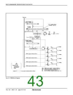
Figure 8.7.1 shows the PWM block diagram. The PWM timing gen-
erating circuit applies individual control signals to PWM0–PWM4 us-
ing f(XIN) divided by 2 as a reference signal.
8.7.1 Data Setting
When outputting DA, first set the high-order 8 bits to the DA-H regis-
ter (address 020616), then the low-order 6 bits to the DA-L register
(address 020716). When outputting PWM0–PWM4, set 8-bit output
data to the PWMi register (i means 0 to 4; addresses 020016 to
020416).
As with 8-bit PWM, set the bit 0 of the PWM mode register 1 (ad-
dress 020816) to “0” (at reset, bit 0 is already set to “0” automati-
cally), so that the PWM count source is supplied. Pin DA is also
used as port P00. Select output mode by setting bit 0 of the port P0
direction register. Next, select the output polarity by bit 4 of the
PWM mode register 1. Then, the 14-bit PWM outputs from the D-A
output pin by setting bit 5 of the PWM mode register 2 (address
020916)to “1” (at reset, this bit already set to “0” automatically) to
select the DA output.
8.7.2 Transmitting Data from Register to PWM
circuit
Data transfer from the 8-bit PWM register to the 8-bit PWM circuit is
executed when writing data to the register.
The signal output from the 8-bit PWM output pin corresponds to the
contents of this register.
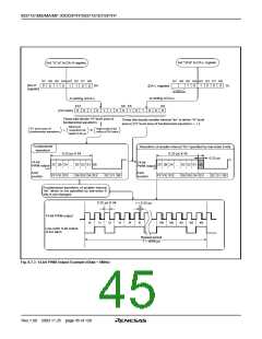
The output example of the 14-bit PWM is shown in Figure 19.The
14-bit PWM divides the data of the DA latch into the low-order 6
bits and the high-order 8 bits.
The fundamental waveform is determined with the high-order 8-bit
data “DH.” A “H” level area with a length τ ✕ DH(“H” level area of
fundamental waveform) is output every short area of “t” = 256τ =
64 µs (τ is the minimum resolution bit width of 0.25 µs). The “H”
level area increase interval (tm) is determined with the low-order 6-
bit data “DL.” The “H” level are of smaller intervals “tm” shown in
Table.8.7.1 is longer by τ than that of other smaller intervals in
PWM repeat period “T” = 64t. Thus, a rectangular waveform with
the different “H” width is output from the D-A pin. Accordingly, the
PWM output changes by τ unit pulse width by changing the con-
tents of the DA-H and DA-L registers. A length of entirely “H” out-
put cannot be output, i. e. 256/256.
Also, data transfer from the DA register (addresses 020616 and
020716) to the 14-bit PWM circuit is executed at writing data to the
DA-L register (address 020716). Reading from the DA-H register (ad-
dress 020616) means reading this transferred data. Accordingly, it is
possible to confirm the data being output from the D-A output pin by
reading the DA register.
8.7.3 Operating of PWM
The following explains the PWM operation.
• 8bit PWM Operation
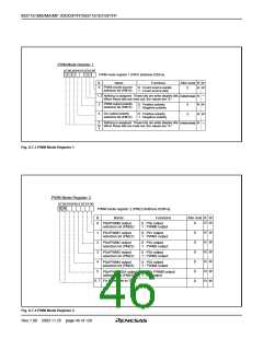
First, set bit 0 of PWM mode register 1 (address 020816) to “0” (at
reset, bit 0 is already set to “0” automatically), so that the PWM
count source is supplied.
PWM0–PWM4 are also used as pins P00–P04. Set the correspond-
ing bits of the port P0 direction register to “1” (output mode). And
select each output polarity by bit 3 of PWM mode register 1 (ad-
dress 020816). Then, set bits 4 to 0 of PWM mode register 2 (ad-
dress 020916) to “1” (PWM output).
Table 8.7.1
Relation Between Low-order 6-bit Data and High-
level Area Increase Interval
Low-order 6 bits of Data Area Longer by t Than That of Other tm (m = 0 to 63)
LSB
The PWM waveform is output from the PWM output pins by set-
ting these registers.
0 0 0 0 0 0
0 0 0 0 0 1
0 0 0 0 1 0
0 0 0 1 0 0
0 0 1 0 0 0
0 1 0 0 0 0
1 0 0 0 0 0
Nothing
m = 32
m = 16, 48
m = 8, 24, 40, 56
m = 4, 12, 20, 28, 36, 44, 52, 60
m = 2, 6, 10, 14, 18, 22, 26, 30, 34, 38, 42, 46, 50, 54, 58, 62
m = 1, 3, 5, 7, ...................................... 57, 59, 61, 63
8.7.4 Output after Reset
At reset, the output of ports P00–P04 is in the high-impedance state,
and the contents of the PWM register and the PWM circuit are unde-
fined. Note that after reset, the PWM output is undefined until setting
the PWM register.
Rev.1.00 2003.11.25 page 42 of 128

 RENESAS [ RENESAS TECHNOLOGY CORP ]